Basic Electronics: Semiconductors
In 1839, Becquerel discovered that some materials generate an electric current when exposed to light. This is known as the photoelectric effect and is the basis of operations of solar cells. Solar cells are made of semiconductors.
- Note: Semiconductors are materials that act as insulators at low temperatures, but as conductors when energy or heat is available.
At present, most solar cells are silicon-based, since this is the most mature technology. However, other materials are under active investigation and may supersede silicon in the long term. The electrical properties of semiconductors can be explained using two models, the bond and the band models.
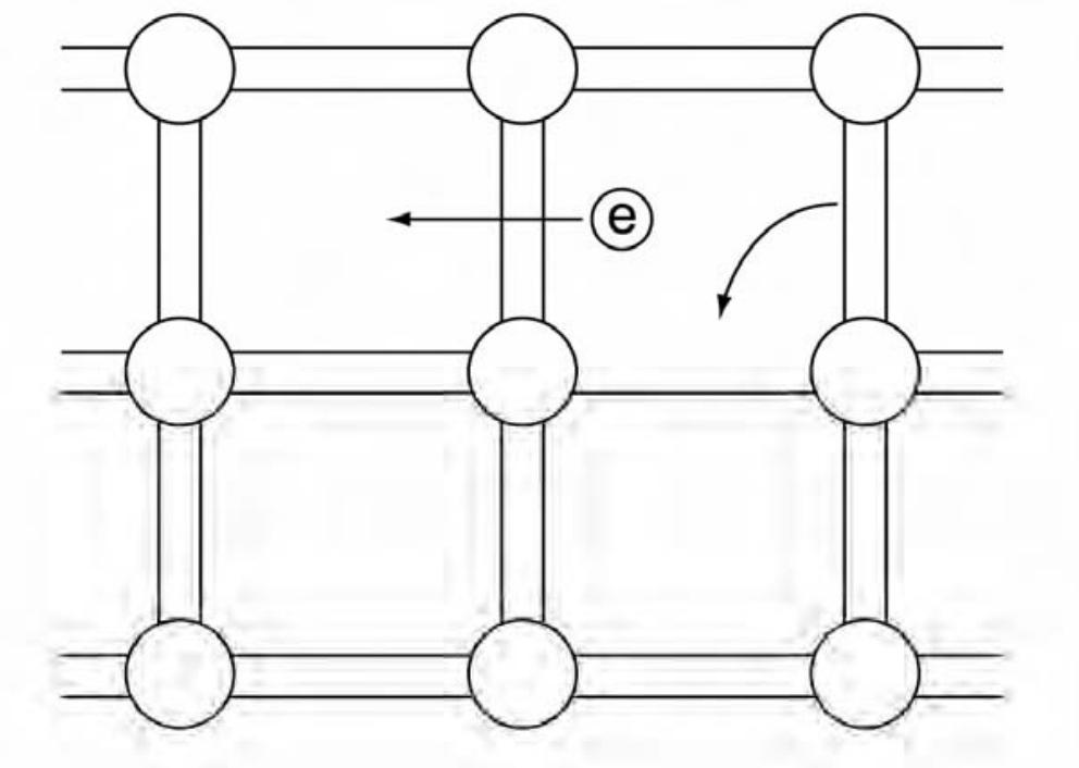
- The bond model uses the covalent bonds joining the silicon atoms to describe semiconductor behaviour. At low temperatures, silicon acts as an insulator because the bonds are intact. At high temperatures, some bonds break, allowing conduction through two processes:
- Electrons from broken bonds are free to move.
- Electrons from neighboring bonds can move into the ‘hole’ created by the broken bond, causing the hole to propagate as if it had a positive charge.
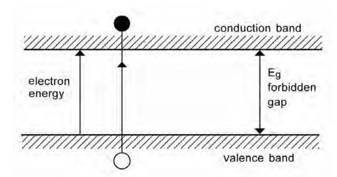
- The band model describes semiconductor behaviour in terms of the energy levels between valence and conduction bands. The electrons in covalent bonds have energies corresponding to those in the valence band. In the conduction band the electrons are free. The forbidden gap corresponds to the minimum energy needed to release an electron from a covalent bond to the conducting band where it can conduct a current. The holes remaining conduct in the opposite direction in the valence band, as described for the bond model.
Doping
It is possible to shift the balance of electrons and holes in a silicon crystal lattice by ‘doping’ it with other atoms. Atoms with one more valence electron than the semiconductor are used to produce ‘n-type’ material. Atoms with one less valence electron result in ‘p-type’ material.
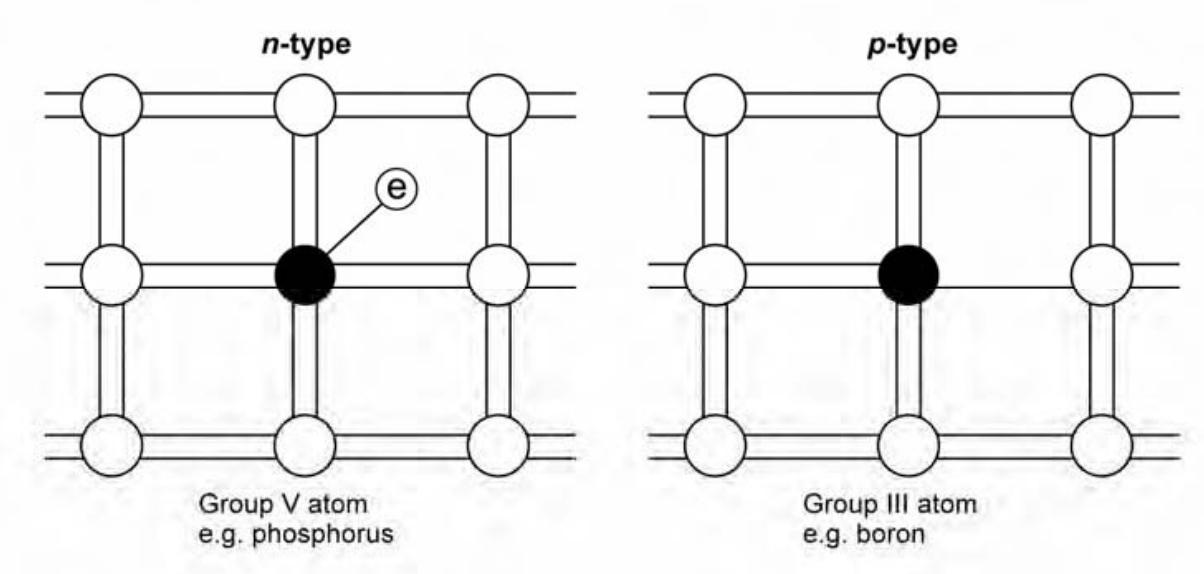
The digram below shows the classification of semiconductors based on doping.
- Intrinsic Semiconductors: Pure semiconductors are called intrinsic semiconductors. They are made of silicon or germanium. They have equal numbers of electrons and holes.
- Extrinsic Semiconductors: Semiconductors doped with impurities are called extrinsic semiconductors. They are of two types: n-type and p-type.
PN Junction
A PN junction is formed by joining a p-type and an n-type semiconductor. The junction has a depletion region where the electrons and holes have combined, leaving behind immobile ions. The depletion region acts as an insulator, preventing current flow. When a voltage is applied across the junction, the depletion region narrows, allowing current to flow. The junction is used in diodes, transistors, and solar cells. Figure below shows the formation of a PN junction.
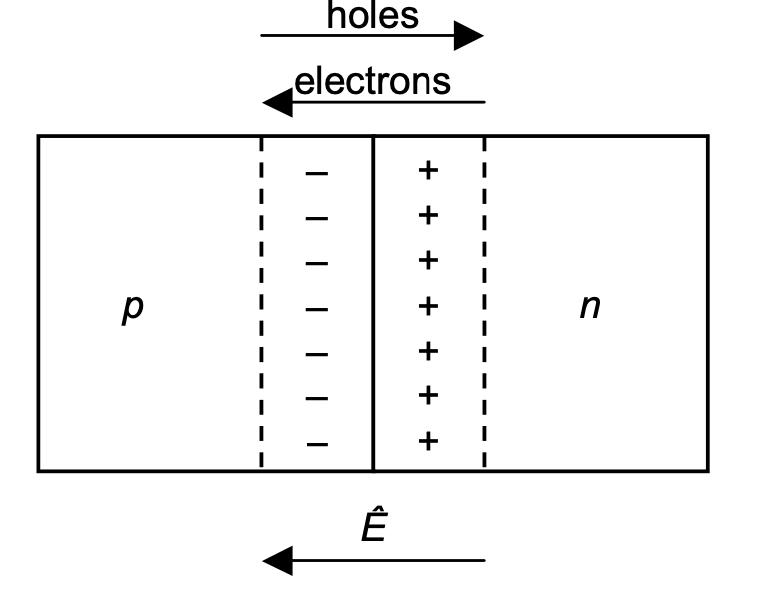
Mechanism of Formation of PN Junction: When a p-type semiconductor and an n-type semiconductor are brought into contact, electrons from the n-type region diffuse into the p-type region and recombine with holes. Similarly, holes from the p-type region diffuse into the n-type region and recombine with electrons. This diffusion process continues until a depletion region is formed at the junction, where no free charge carriers are present. The immobile ions left behind create an electric field that opposes further diffusion of charge carriers. This electric field establishes a built-in potential barrier that must be overcome for current to flow across the junction. When an external voltage is applied, it can either widen or narrow the depletion region, allowing or preventing current flow, respectively.
Based on the voltage applied, the PN junction can be classified into three modes of operation:
- Forward Bias: When the positive terminal of the battery is connected to the p-type region and the negative terminal to the n-type region, the depletion region narrows, allowing current to flow. This is the forward bias mode.
- Reverse Bias: When the positive terminal of the battery is connected to the n-type region and the negative terminal to the p-type region, the depletion region widens, preventing current flow. This is the reverse bias mode.
- Zero Bias: When no external voltage is applied, the depletion region remains constant, and no current flows. This is the zero bias mode.
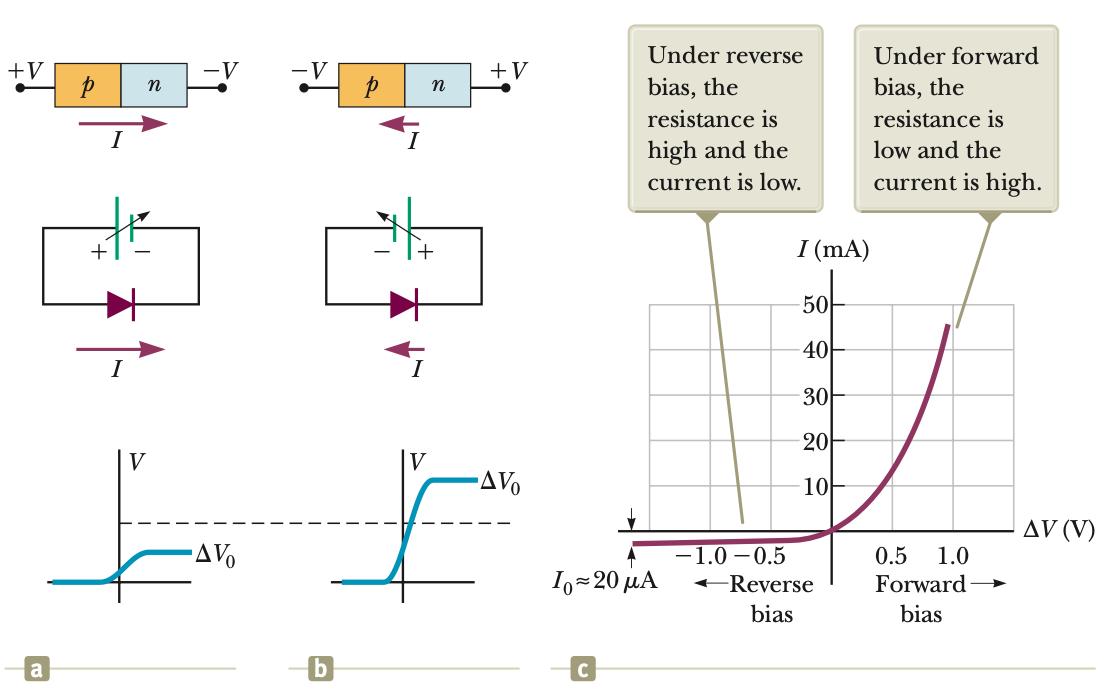
The operation of a junction as a diode is best understood in terms of the potential difference graph shown at the bottom of Figure-(a,b,c) above. When a voltage $\Delta V$ is applied to the junction such that the $p$-side is connected to the positive terminal of a voltage source (as shown in Figure-a), the internal potential difference $\Delta V_0$ across the junction decreases, as illustrated at the bottom of the figure. This decrease results in a current that increases exponentially with increasing forward voltage (or forward bias). In the case of reverse bias—where the $n$-side of the junction is connected to the positive terminal of a voltage source—the internal potential difference $\Delta V_0$ increases with increasing reverse bias, as shown in Figure-b. This increase leads to a very small reverse current that quickly reaches a saturation value, $I_0$. The current–voltage relationship for an ideal diode is given by the equation:
$I = I_0 \left(e^{\frac{e \Delta V}{k_B T}} - 1\right)$,
where the first $e$ is the base of the natural logarithm, the second $e$ represents the magnitude of the electron charge, $k_B$ is Boltzmann’s constant, and $T$ is the absolute temperature. Figure-c shows an $I$–$\Delta V$ plot characteristic of a real $p$–$n$ junction, demonstrating its one-way valve behavior.
Exercise
- Estimate the band gap of the semiconductor in the infrared LED of a typical television remote control. Hint: the wavelength of infrared light ranges from 700 nm to 1 mm.