

29 Jul 2025
BJT DC Load Line and Q-Point
Collector-circuit constraint, characteristic intersection, bias point, and allowable signal swing.
For a grounded-emitter CE circuit with collector resistance $R_C$ and dc supply $V_{CC}$,
\[V_{CC}=I_CR_C+V_{CE}.\]Therefore every allowed dc state must lie on
\[\boxed{I_C=\frac{V_{CC}-V_{CE}}{R_C}}.\]This is the dc load line. Its endpoints in the idealized model are
\[(V_{CE},I_C)=(V_{CC},0) \quad\text{and}\quad (0,V_{CC}/R_C).\]The first is the cutoff endpoint; the second approximates saturation. A real saturated transistor instead has $V_{CE}=V_{CE(sat)}>0$, so the maximum current is approximately $(V_{CC}-V_{CE(sat)})/R_C$.
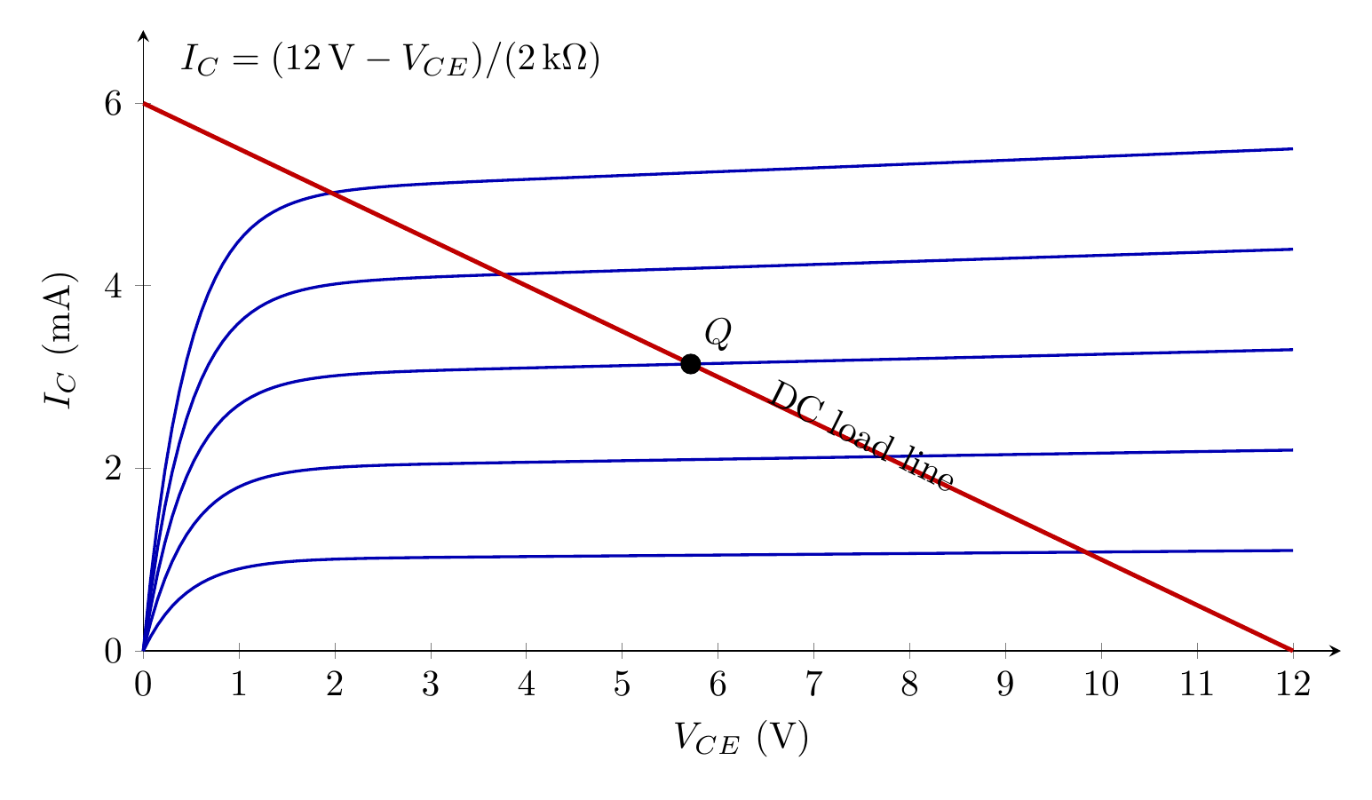
The editable source is transistor-characteristics.tex.
The base-bias circuit selects one output curve. Its intersection with the load line is the quiescent point
\[Q=(V_{CEQ},I_{CQ}).\]For a simple fixed base supply $V_{BB}$ and base resistance $R_B$,
\[I_{BQ}\simeq\frac{V_{BB}-V_{BEQ}}{R_B},\]provided $V_{BB}>V_{BEQ}$. The transistor characteristic, not the approximation $I_C=\beta I_B$ alone, determines the final $Q$.
An ac input moves the instantaneous operating point along the same dc load line. To avoid clipping, it must remain between cutoff and saturation. In the idealized resistor-loaded circuit, a roughly symmetric voltage swing is obtained near
\[V_{CEQ}\simeq\frac{V_{CC}}2, \qquad I_{CQ}\simeq\frac{V_{CC}}{2R_C}.\]These midpoint formulas are not universal: emitter resistance, transformer loading, finite $V_{CE(sat)}$, and nonlinear characteristic spacing shift the best bias point. If an emitter resistor $R_E$ is present,
\[V_{CC}=I_CR_C+V_{CE}+I_ER_E,\]and $I_E\simeq I_C$ is an additional large-$\beta$ approximation.
Solved Problems
1. Locate an active-region Q-point
An npn CE circuit has $V_{CC}=12.0\,\mathrm V$, $R_C=2.00\,\mathrm{k\Omega}$, $\beta=80$, and $I_B=40.0\,\mu\mathrm A$. Neglect leakage and first test the active-region model.
\[I_{CQ}=\beta I_B=(80)(40.0\,\mu\mathrm A)=3.20\,\mathrm{mA}.\]The load line then gives
\[V_{CEQ}=V_{CC}-I_{CQ}R_C =12.0-(3.20\,\mathrm{mA})(2.00\,\mathrm{k\Omega}) =5.60\,\mathrm V.\]This is well above a typical $V_{CE(sat)}$, so the assumed active region is self-consistent. The transistor dissipation is $P_Q=V_{CEQ}I_{CQ}=17.9\,\mathrm{mW}$, and the circuit check is $5.60\,\mathrm V+6.40\,\mathrm V=12.0\,\mathrm V$.
2. Load line of a Thevenin collector network
A grounded-emitter transistor has its collector connected to $+12.0\,\mathrm V$ through $4.00\,\mathrm{k\Omega}$ and to ground through $12.0\,\mathrm{k\Omega}$. Reduce the surrounding collector network to its Thevenin equivalent and obtain the dc load line.
With the transistor port open, the divider voltage is
\[V_{th}=12.0\frac{12.0}{4.00+12.0}=9.00\,\mathrm V.\]Suppressing the ideal supply gives
\[R_{th}=4.00\,\mathrm{k\Omega}\mathbin{\|}12.0\,\mathrm{k\Omega} =3.00\,\mathrm{k\Omega}.\]The collector port therefore obeys
\[\boxed{V_{CE}=9.00-(3.00\,\mathrm{k\Omega})I_C}.\]Its intercepts are $(V_{CE},I_C)=(9.00\,\mathrm V,0)$ and $(0,3.00\,\mathrm{mA})$. The reduction shows that a multi-resistor collector network still produces a straight load line, but with its Thevenin voltage and resistance.
3. Center a voltage swing with finite saturation voltage
A $9.00\,\mathrm V$ supply must bias a transistor at $I_{CQ}=2.00\,\mathrm{mA}$. Take $V_{CE(sat)}=0.20\,\mathrm V$ and center the Q-point between cutoff and saturation in voltage.
The usable interval is $0.20\,\mathrm V\le V_{CE}\le9.00\,\mathrm V$, so
\[V_{CEQ}=\frac{9.00+0.20}{2}=4.60\,\mathrm V.\]Then
\[R_C=\frac{V_{CC}-V_{CEQ}}{I_{CQ}} =\frac{9.00-4.60}{2.00\,\mathrm{mA}} =2.20\,\mathrm{k\Omega}.\]Both voltage margins are $4.40\,\mathrm V$, so the chosen point provides equal idealized positive and negative collector-voltage swing.
Descriptive Questions
- Derive the dc load-line equation and explain the physical meaning of its two intercepts.
- Explain how a transistor output characteristic and an external collector circuit jointly determine the Q-point.
- Discuss why a midpoint Q-point is useful for undistorted signal swing and why it is not universal.
- Explain how an emitter resistor modifies the collector-circuit load line and improves bias stability.
Numerical Problems
-
Draw the intercept data for $V_{CC}=15.0\,\mathrm V$ and $R_C=3.00\,\mathrm{k\Omega}$.
Final answer: Cutoff intercept $(V_{CE},I_C)=(15.0\,\mathrm V,0)$ and ideal saturation-axis intercept $(0,5.00\,\mathrm{mA})$; slope $-1/R_C=-0.333\,\mathrm{mA\,V^{-1}}$.
-
A measured collector load line passes through $(V_{CE},I_C)=(2.00\,\mathrm V,4.00\,\mathrm{mA})$ and $(8.00\,\mathrm V,1.00\,\mathrm{mA})$. Infer $R_C$ from the slope and then reconstruct $V_{CC}$.
Final answer: The slope is $-0.500\,\mathrm{mA\,V^{-1}}$, so $R_C=2.00\,\mathrm{k\Omega}$ and $V_{CC}=V_{CE}+I_CR_C=10.0\,\mathrm V$ from either point.
-
A transistor has the dc load line $I_C=(12.0-V_{CE})/(2.00\,\mathrm{k\Omega})$ and a dissipation limit $P_D=16.0\,\mathrm{mW}$. Find the two intersections of the load line with the constant-power boundary $V_{CE}I_C=P_D$, and identify the load-line interval that violates the limit.
Final answer: $V_{CE}(12.0-V_{CE})=32.0$ gives $V_{CE}=4.00\,\mathrm V$ with $I_C=4.00\,\mathrm{mA}$ and $V_{CE}=8.00\,\mathrm V$ with $I_C=2.00\,\mathrm{mA}$. The segment $4.00<V_{CE}<8.00\,\mathrm V$ exceeds $16.0\,\mathrm{mW}$.
-
A circuit contains $R_C=2.00\,\mathrm{k\Omega}$ and $R_E=1.00\,\mathrm{k\Omega}$ in series with a $12.0\,\mathrm V$ supply. If $I_C\simeq I_E=3.00\,\mathrm{mA}$, find $V_{CE}$.
Final answer: $V_{CE}=12.0-(3.00\,\mathrm{mA})(2.00+1.00)\,\mathrm{k\Omega}=3.00\,\mathrm V$; the two resistor drops total $9.00\,\mathrm V$.
The load-line identities, region tests, and numerical results are reproducible in bjt-load-line-check.mac; every printed residual is zero.


Discussion