

27 Jul 2025
BJT Operation, Current Flow, and Regions
npn and pnp transistor structure, carrier transport, terminal currents, and active, cutoff, and saturation regions.
A bipolar junction transistor has two p-n junctions sharing a thin base. In an npn device the emitter is heavily doped n-type, the base is thin and lightly doped p-type, and the collector is moderately doped n-type with a larger area for voltage and heat handling. A pnp device reverses every semiconductor type and operating polarity.
Forward-active npn transport
Define
\[V_{BE}=V_B-V_E, \qquad V_{BC}=V_B-V_C.\]Forward-active operation has the emitter-base junction forward biased, $V_{BE}>0$, and the base-collector junction reverse biased, $V_{BC}<0$. The precise forward voltage is current- and temperature-dependent; $0.6$–$0.8\,\mathrm V$ is only a common silicon range, not a mathematical boundary.
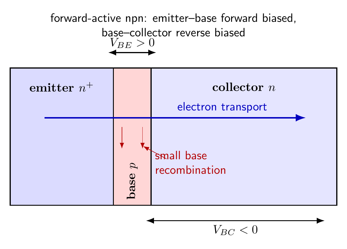
The editable source is bjt-operation.tex.
Electrons injected from the emitter become minority carriers in the base. Because the neutral base width is much smaller than their diffusion length, most diffuse to the collector depletion layer and are swept into the collector. The smaller recombination fraction must be replaced through the base terminal and forms base current. Hole injection from base to emitter is kept small by the emitter’s much heavier doping.
For an npn transistor, conventional $I_C$ and $I_B$ enter collector and base while $I_E$ leaves the emitter. Using positive current magnitudes,
\[\boxed{I_E=I_C+I_B}.\]The common-base transport factor is
\[\alpha_F=\frac{I_C}{I_E}, \qquad 0<\alpha_F<1,\]when leakage is neglected. Efficient emitter injection and little base recombination make $\alpha_F$ close to unity. The corresponding common-emitter gain is
\[I_C\simeq\beta_F I_B, \qquad \beta_F=\frac{\alpha_F}{1-\alpha_F}.\]These are operating-point parameters, not universal material constants.
Operating regions
The junction biases determine the region for an npn transistor:
| Region | Emitter-base junction | Base-collector junction | Behaviour |
|---|---|---|---|
| Cutoff | reverse or not appreciably forward biased | reverse biased | $I_B\simeq0$ and $I_C$ is leakage-scale |
| Forward active | forward biased | reverse biased | $I_C\simeq\beta_FI_B$; amplification region |
| Saturation | forward biased | forward biased | both junctions inject; $I_C$ is circuit-limited |
| Reverse active | reverse biased | forward biased | emitter and collector exchange roles; gain is usually lower |
In saturation, increasing $I_B$ no longer produces the active-region value $\beta_FI_B$ because the external collector circuit limits current. $V_{CE}$ then approaches a small positive $V_{CE(sat)}$ for npn operation rather than becoming exactly zero.
For a pnp transistor, holes are the principal injected carriers. Conventional currents and all voltage polarities reverse: forward-active operation requires $V_{BE}<0$ and $V_{BC}>0$. The same magnitude relations $I_E=I_C+I_B$ and $0<\alpha_F<1$ apply.
Solved Problems
1. Currents from the common-base transport factor
An npn transistor operates in the forward-active region with $\alpha_F=0.985$ and $I_E=4.00\,\mathrm{mA}$. Find $I_C$, $I_B$, and $\beta_F$.
Using the definitions,
\[I_C=\alpha_F I_E=(0.985)(4.00\,\mathrm{mA})=3.94\,\mathrm{mA},\] \[I_B=I_E-I_C=4.00-3.94=0.0600\,\mathrm{mA}=60.0\,\mu\mathrm A.\]Hence
\[\beta_F=\frac{I_C}{I_B}=\frac{3.94}{0.0600}=65.7.\]The sign convention is consistent: $I_C$ and $I_B$ enter the device while $I_E$ leaves it. The current check is $3.94\,\mathrm{mA}+0.0600\,\mathrm{mA}=4.00\,\mathrm{mA}$.
2. Region identification from terminal voltages
For an npn transistor, $V_E=0$, $V_B=0.72\,\mathrm V$, and $V_C=5.00\,\mathrm V$. Its measured currents are $I_C=2.50\,\mathrm{mA}$ and $I_B=50.0\,\mu\mathrm A$. Identify the region and calculate $I_E$, $\alpha_F$, and $\beta_F$.
The junction voltages are
\[V_{BE}=V_B-V_E=+0.72\,\mathrm V, \qquad V_{BC}=V_B-V_C=-4.28\,\mathrm V.\]Thus the emitter-base junction is forward biased and the base-collector junction is reverse biased: the transistor is forward active. Also,
\[I_E=I_C+I_B=2.50\,\mathrm{mA}+0.0500\,\mathrm{mA}=2.55\,\mathrm{mA},\] \[\alpha_F=\frac{2.50}{2.55}=0.9804, \qquad \beta_F=\frac{2.50\,\mathrm{mA}}{50.0\,\mu\mathrm A}=50.0.\]The independent identity $\alpha_F=\beta_F/(\beta_F+1)=50/51=0.9804$ checks the result.
Descriptive Questions
- Explain why a BJT emitter is heavily doped, its base is thin and lightly doped, and its collector is comparatively wide.
- Describe electron transport and conventional-current directions in a forward-active npn transistor.
- Distinguish cutoff, forward-active, saturation, and reverse-active operation using the two junction biases.
- Explain why transistor saturation does not mean that the collector current is intrinsically zero or fixed.
Numerical Problems
-
In a forward-active npn transistor, the emitter injects $4.90\,\mathrm{mA}$ of electron current into the base while the base injects $0.100\,\mathrm{mA}$ of hole current into the emitter. If $2.00\%$ of the injected electron current recombines in the base, resolve the collector and base currents and find the emitter injection efficiency and base transport factor.
Final answer: $I_C=4.802\,\mathrm{mA}$, $I_B=0.198\,\mathrm{mA}$, $\gamma_E=4.90/5.00=0.9800$, and $\alpha_T=0.9800$; $I_C+I_B=5.000\,\mathrm{mA}$.
-
A common-base measurement gives $I_E=2.00\,\mathrm{mA}$ and $I_C=1.970\,\mathrm{mA}$. If the forward transport factor is independently known to be $\alpha_F=0.980$, use $I_C=\alpha_FI_E+I_{CBO}$ to extract the collector-base leakage current and then apply KCL to find $I_B$.
Final answer: $I_{CBO}=10.0\,\mu\mathrm A$ and $I_B=I_E-I_C=30.0\,\mu\mathrm A$.
-
An npn stage has $V_E=0.20\,\mathrm V$ and $V_B=0.90\,\mathrm V$. To keep it forward active with at least $2.00\,\mathrm V$ of reverse bias across the base-collector junction, find the minimum collector voltage and the corresponding minimum $V_{CE}$.
Final answer: Requiring $V_C-V_B\ge2.00\,\mathrm V$ gives $V_C\ge2.90\,\mathrm V$ and $V_{CE}\ge2.70\,\mathrm V$; meanwhile $V_{BE}=+0.70\,\mathrm V$.
-
An npn transistor with nominal $\beta_F=80$ is driven with $I_B=100\,\mu\mathrm A$ through $R_C=1.00\,\mathrm{k\Omega}$ from $V_{CC}=5.00\,\mathrm V$. Take $V_{CE(sat)}=0.20\,\mathrm V$. Decide whether it is active or saturated and find the forced current gain.
Final answer: Active-mode prediction $I_C=8.00\,\mathrm{mA}$ exceeds the circuit limit $(5.00-0.20)/1.00\,\mathrm{k\Omega}=4.80\,\mathrm{mA}$; it is saturated and $I_C/I_B=48.0$.
The algebra and numerical values are reproducible in bjt-operation-check.mac; every printed residual is zero.


Discussion