

27 Jun 2025
Diode Load Line and Rectifier Circuits
Diode operating point, half-wave rectification, and center-tapped and bridge full-wave rectifiers.
For a diode in series with a resistance $R_L$ and an instantaneous source voltage $V_s$, Kirchhoff’s voltage law gives
\[V_s=V_D+IR_L,\]or
\[\boxed{I=\frac{V_s-V_D}{R_L}}.\]This straight load line has slope $-1/R_L$ on an $I$ versus $V_D$ graph. Its intersection with the nonlinear diode characteristic is the operating or quiescent point $Q$. With an ac source the load line changes with time, so the operating point moves along the diode curve.
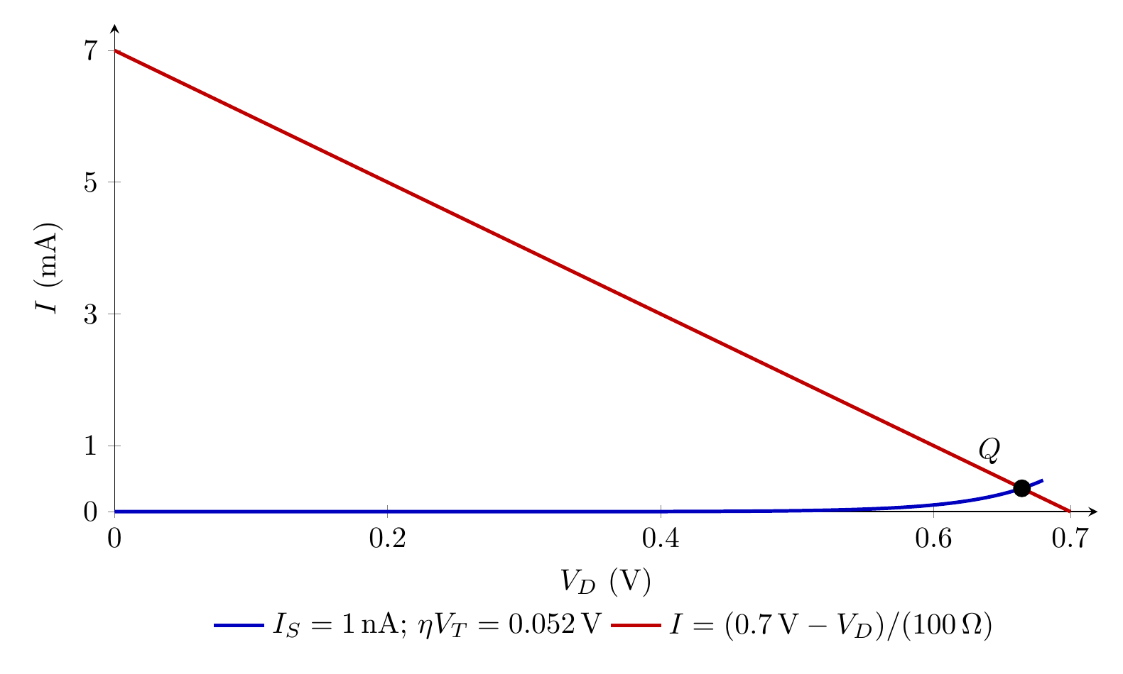
The editable source is diode-load-line.tex.
Half-wave rectifier
Let the secondary voltage be $v_s=V_m\sin\theta$, where $\theta=\omega t$. With an ideal series diode and a resistive load,
\[v_o(\theta)= \begin{cases} V_m\sin\theta,&0<\theta<\pi,\\ 0,&\pi<\theta<2\pi, \end{cases}\]repeated every $2\pi$. The diode conducts during the positive half-cycle and blocks during the negative half-cycle. With a constant forward drop $V_F$, conduction occurs only where $v_s>V_F$ and $v_o\simeq v_s-V_F$.
The ideal peak inverse voltage of the half-wave diode is $V_m$.
Center-tapped full-wave rectifier
The two ends of a center-tapped secondary have opposite voltages relative to the centre tap. If the peak voltage of each half-secondary is called $V_m$, one diode conducts on each half-cycle while the other is reverse biased. Both paths drive load current in the same direction, giving ideally
\[\boxed{v_o=V_m\lvert\sin\theta\rvert}.\]Only one diode drop lies in the conducting path. The ideal peak inverse voltage across the nonconducting diode is $2V_m$.
Bridge full-wave rectifier
A bridge uses four diodes. One diagonal pair conducts for $v_s>0$ and the other for $v_s<0$, so the load polarity is unchanged:
\[\boxed{v_o=\lvert v_s\rvert=V_m\lvert\sin\theta\rvert}.\]Two diode drops occur in series; the constant-drop model gives $v_o\simeq\max(\lvert v_s\rvert-2V_F,0)$. Here $V_m$ is the peak of the complete transformer secondary, and the ideal peak inverse voltage per diode is $V_m$.
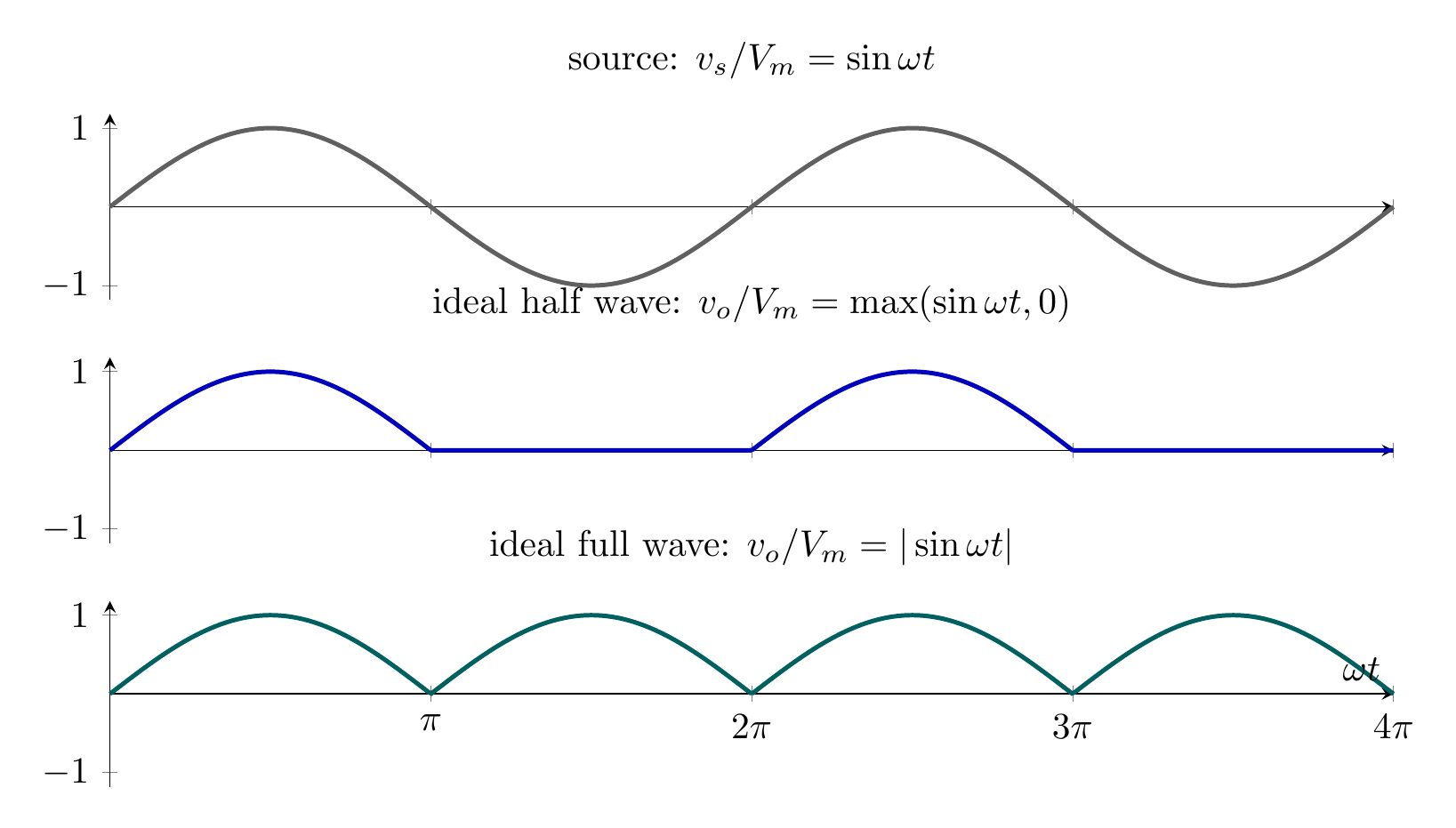
The editable source is rectifier-waveforms.tex.
Solved Problems
1. Diode Q-point in the constant-drop model
A $5.00\,\mathrm V$ source drives a silicon diode through $R_L=1.00\,\mathrm{k\Omega}$. Approximate the forward drop by $V_F=0.700\,\mathrm V$.
The conducting load line is
\[I=\frac{5.00-V_D}{1.00\,\mathrm{k\Omega}}.\]At the constant-drop intersection $V_D=0.700\,\mathrm V$,
\[I_Q=\frac{5.00-0.700}{1.00\,\mathrm{k\Omega}}=4.30\,\mathrm{mA}.\]Thus $Q=(0.700\,\mathrm V,4.30\,\mathrm{mA})$. The voltage check is $0.700\,\mathrm V+(4.30\,\mathrm{mA})(1.00\,\mathrm{k\Omega})=5.00\,\mathrm V$. If the nonlinear diode curve is used instead, its intersection replaces this approximation.
2. Conduction interval of a half-wave rectifier
Let $v_s=10.0\sin\theta\,\mathrm V$, $V_F=0.700\,\mathrm V$, and $R_L=1.00\,\mathrm{k\Omega}$. Conduction begins when $v_s=V_F$:
\[\theta_0=\sin^{-1}\!\left(\frac{0.700}{10.0}\right)=0.07006\,\mathrm{rad}=4.014^\circ.\]The diode conducts for $\theta_0<\theta<\pi-\theta_0$. At the crest,
\[I_{L,\max}=\frac{10.0-0.700}{1.00\,\mathrm{k\Omega}}=9.30\,\mathrm{mA}.\]On the negative crest it blocks approximately $10.0\,\mathrm V$, so its required PIV rating must exceed $V_m$ with an engineering safety margin.
3. Centre-tapped and bridge transformer requirements
Suppose the required peak load voltage is $12.0\,\mathrm V$ and each conducting diode drops $0.700\,\mathrm V$.
For a centre-tapped rectifier, only one diode conducts, so each half-secondary needs
\[V_{m,\text{half}}=12.0+0.700=12.7\,\mathrm V,\]and the nonconducting diode sees approximately
\[\mathrm{PIV}=2V_{m,\text{half}}=25.4\,\mathrm V.\]For a bridge, two diodes conduct, so the complete secondary needs
\[V_{m,\text{bridge}}=12.0+2(0.700)=13.4\,\mathrm V,\]while each idealized diode sees approximately $13.4\,\mathrm V$ PIV. The bridge uses the full secondary each half-cycle but loses two forward drops.
Descriptive Questions
- Explain the graphical diode load-line construction and the meaning of its intersection with the diode characteristic.
- Describe half-wave rectifier operation over one complete source cycle, including the diode PIV.
- Compare centre-tapped and bridge full-wave rectifiers in transformer use, conducting diode count, voltage drop, and PIV.
- Explain why full-wave rectification doubles ripple frequency without doubling the supply frequency.
Numerical Problems
-
A manufacturer’s diode curve identifies the desired operating point as $Q=(V_D,I)=(0.800\,\mathrm V,12.0\,\mathrm{mA})$. From a $5.00\,\mathrm V$ source, choose the required series resistance. Also find its dissipation at $Q$ and the load line’s current-axis intercept.
Final answer: $R_L=(5.00-0.800)/(12.0\,\mathrm{mA})=350\,\Omega$. Its dissipation is $P_R=I^2R_L=50.4\,\mathrm{mW}$, and the current-axis intercept is $V_s/R_L=14.29\,\mathrm{mA}$.
-
A half-wave rectifier has $v_s=10.0\sin\theta\,\mathrm V$, $V_F=0.600\,\mathrm V$, and $R_L=880\,\Omega$. Find $(v_o,i_L,v_D)$ at $\theta=\pi/6$ and $7\pi/6$, taking $v_D=v_A-v_K$.
Final answer: At $\pi/6$, the diode conducts: $v_o=4.40\,\mathrm V$, $i_L=5.00\,\mathrm{mA}$, and $v_D=+0.600\,\mathrm V$. At $7\pi/6$ it is off: $v_o=i_L=0$ and $v_D=-5.00\,\mathrm V$, a $5.00\,\mathrm V$ reverse bias.
-
A $50.0\,\mathrm{Hz}$ centre-tapped full-wave rectifier has $10.0\,\mathrm V$ peak from each half-secondary, $V_F=0.700\,\mathrm V$, and $R_L=930\,\Omega$. One rectifier diode fails open. Find the surviving output peak, peak load current, and output-pulse repetition rate.
Final answer: The circuit becomes half-wave: $V_{o,\mathrm{pk}}=10.0-0.700=9.30\,\mathrm V$, $I_{L,\mathrm{pk}}=9.30/930=10.0\,\mathrm{mA}$, and the pulses repeat at $50.0\,\mathrm{Hz}$, not $100\,\mathrm{Hz}$.
-
A bridge has source-crest magnitude $12.0\,\mathrm V$ and $R_L=1.00\,\mathrm{k\Omega}$. The conducting pair on the positive crest drops $0.600\,\mathrm V$ and $0.700\,\mathrm V$; the negative-crest pair drops $0.750\,\mathrm V$ and $0.650\,\mathrm V$. Find the two output-voltage and load-current peaks.
Final answer: Positive crest: $V_{o,\mathrm{pk}}=10.7\,\mathrm V$ and $I_{L,\mathrm{pk}}=10.7\,\mathrm{mA}$. Negative crest: $V_{o,\mathrm{pk}}=10.6\,\mathrm V$ and $I_{L,\mathrm{pk}}=10.6\,\mathrm{mA}$. Both currents have the same load direction; the $0.100\,\mathrm V$ height difference comes from the unequal pair drops.
The load-line constraints, conduction boundary, PIV relations, and all numerical values are reproducible in diode-load-line-rectifiers-check.mac; every printed residual is zero.


Discussion