

30 Jul 2025
FETs and JFET Characteristics
Field-effect control, n- and p-channel JFET operation, output regions, transfer law, and device parameters.
A field-effect transistor controls current in a semiconductor channel by an electric field. Conduction uses majority carriers, and the control terminal draws very little dc current. A JFET forms its gate from a reverse-biased p-n junction.
n-channel JFET operation
An n-type channel joins source to drain and p-type gate regions contact its sides. Use
\[V_{DS}=V_D-V_S\ge0, \qquad V_{GS}=V_G-V_S\le0.\]The reverse-biased gate depletion regions narrow the channel. For small $V_{DS}$ the channel behaves approximately as a voltage-controlled resistor. Because
\[V_{GD}=V_{GS}-V_{DS},\]the gate-drain junction is most reverse biased near the drain, so depletion grows asymmetrically.
Let $V_P=V_{GS(off)}<0$. Pinch-off first occurs at the drain end when
\[V_{GD}=V_P,\]or
\[\boxed{V_{DS,sat}=V_{GS}-V_P}.\]Beyond this boundary the pinch-off point moves slightly toward the source and the added drain voltage falls mainly across the depleted region. Current therefore saturates; pinch-off does not mean zero drain current.
An ideal gradual-channel model gives, for $V_P\le V_{GS}\le0$,
\[I_D=\frac{2I_{DSS}}{V_P^2} \left[(V_{GS}-V_P)V_{DS}-\frac{V_{DS}^2}{2}\right], \quad 0\le V_{DS}\le V_{GS}-V_P,\]and in saturation,
\[\boxed{I_D=I_{DSS}\left(1-\frac{V_{GS}}{V_P}\right)^2}, \quad V_{DS}\ge V_{GS}-V_P.\]At $V_{GS}=0$, $I_D=I_{DSS}$ in saturation. At $V_{GS}\le V_P$, the channel is cut off apart from leakage. At sufficiently large $V_{DS}$, gate-junction breakdown ends the normal saturation region.
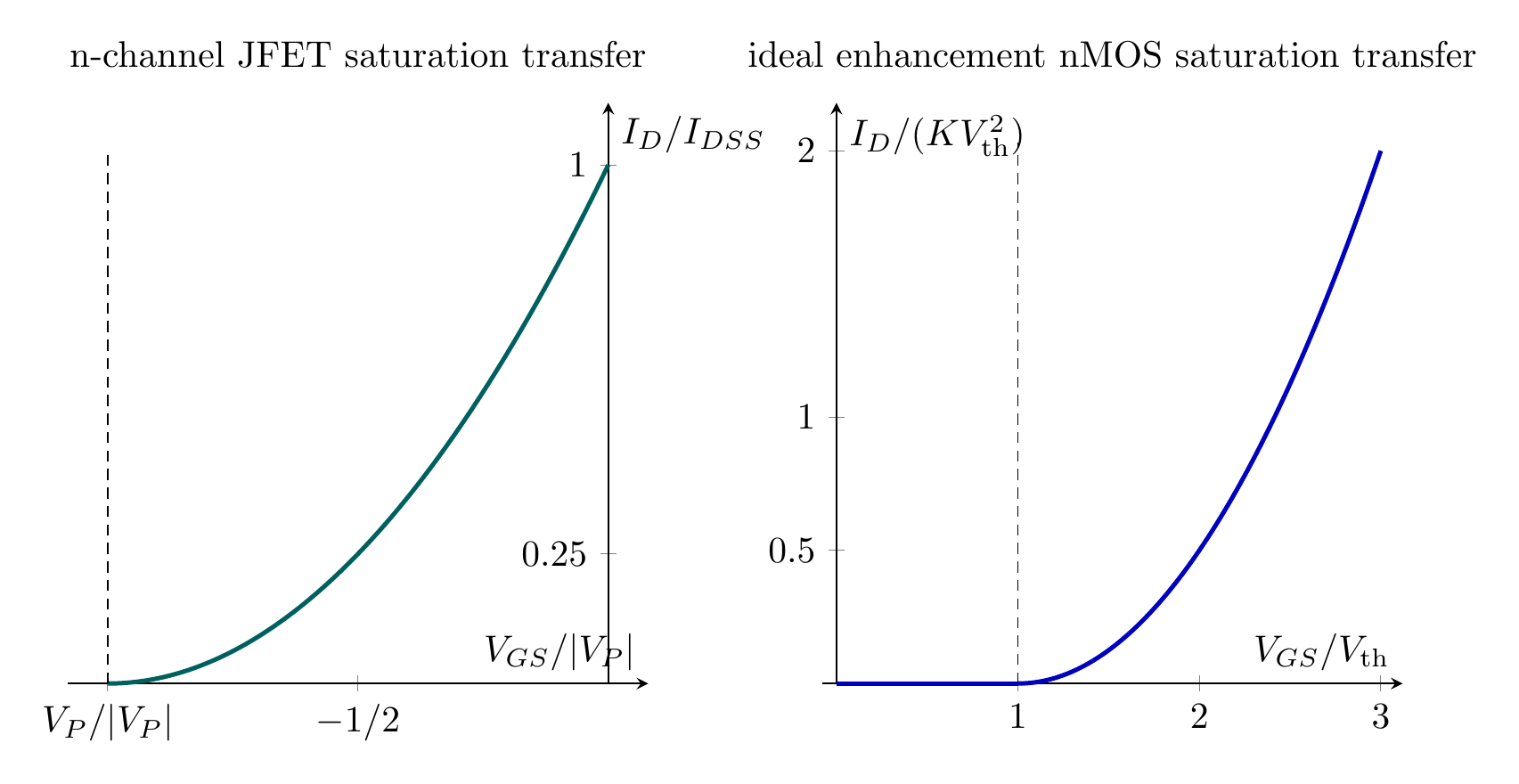
The editable source is fet-transfer.tex.
JFET parameters
At a bias point, the transconductance, drain resistance, and amplification factor are
\[g_m=\left.\frac{\partial I_D}{\partial V_{GS}}\right|_{V_{DS}}, \qquad r_d=\left.\frac{\partial V_{DS}}{\partial I_D}\right|_{V_{GS}},\] \[\mu_F=-\left.\frac{\partial V_{DS}}{\partial V_{GS}}\right|_{I_D} =g_mr_d.\]$g_m$ is in siemens, $r_d$ in ohms, and $\mu_F$ is dimensionless. From Shockley’s transfer law,
\[\boxed{g_m=-\frac{2I_{DSS}}{V_P} \left(1-\frac{V_{GS}}{V_P}\right) =g_{m0}\sqrt{\frac{I_D}{I_{DSS}}}}, \qquad g_{m0}=-\frac{2I_{DSS}}{V_P}>0.\]For a p-channel JFET, holes carry the channel current and all voltage and current polarities reverse. The magnitude characteristics have the same form after consistent sign reversal.
Solved Problems
1. Saturation current, boundary, and transconductance
An n-channel JFET has $I_{DSS}=12.0\,\mathrm{mA}$ and $V_P=-4.00\,\mathrm V$. At $V_{GS}=-1.00\,\mathrm V$, find the saturation current, the onset value of $V_{DS}$, and $g_m$.
The normalized gate factor is
\[1-\frac{V_{GS}}{V_P}=1-\frac{-1.00}{-4.00}=0.750.\]Therefore
\[I_D=12.0(0.750)^2=6.75\,\mathrm{mA},\] \[V_{DS,sat}=V_{GS}-V_P=-1.00-(-4.00)=3.00\,\mathrm V.\]Also $g_{m0}=-2I_{DSS}/V_P=6.00\,\mathrm{mS}$, so
\[g_m=g_{m0}(0.750)=4.50\,\mathrm{mS}.\]All signs are consistent with an n-channel device: $V_P$ and $V_{GS}$ are negative while $V_{DS}$ and the conventional drain-current magnitude are positive.
2. Recover gate bias from drain current
For $I_{DSS}=8.00\,\mathrm{mA}$ and $V_P=-6.00\,\mathrm V$, determine the allowed gate bias when $I_D=2.00\,\mathrm{mA}$ in saturation.
Taking the physical nonnegative square root,
\[\sqrt{\frac{I_D}{I_{DSS}}}=\sqrt{\frac{2.00}{8.00}}=0.500 =1-\frac{V_{GS}}{V_P}.\]Thus
\[V_{GS}=V_P(1-0.500)=-3.00\,\mathrm V.\]The zero-current branch outside $V_P\le V_{GS}\le0$ is not an alternative solution. Here $g_{m0}=2.667\,\mathrm{mS}$ and $g_m=g_{m0}(0.500)=1.333\,\mathrm{mS}$.
3. Current before pinch-off
Take $I_{DSS}=10.0\,\mathrm{mA}$, $V_P=-5.00\,\mathrm V$, $V_{GS}=-1.00\,\mathrm V$, and $V_{DS}=2.00\,\mathrm V$. Since $V_{DS,sat}=4.00\,\mathrm V$, the device is in its voltage-controlled-resistance region. The gradual-channel expression gives
\[I_D=\frac{2(10.0)}{(-5.00)^2} \left[(-1.00+5.00)(2.00)-\frac{(2.00)^2}{2}\right]\mathrm{mA} =4.80\,\mathrm{mA}.\]This is below the saturation value $10.0(1-1/5)^2=6.40\,\mathrm{mA}$, as required before the pinch-off boundary.
Descriptive Questions
- Explain how a reverse-biased gate controls current in an n-channel JFET and why its input resistance is high.
- Derive the pinch-off boundary $V_{DS,sat}=V_{GS}-V_P$ from the gate-drain voltage.
- Distinguish the ohmic, saturation, cutoff, and breakdown regions of a JFET output characteristic.
- Define $g_m$, $r_d$, and $\mu_F$, including their units and the relation among them.
Numerical Problems
-
Transfer measurements on an n-channel JFET give $I_D=9.00\,\mathrm{mA}$ at $V_{GS}=-1.00\,\mathrm V$ and $I_D=1.00\,\mathrm{mA}$ at $V_{GS}=-3.00\,\mathrm V$. Linearize Shockley’s law by plotting $\sqrt{I_D}$ against $V_{GS}$ and extract $I_{DSS}$ and $V_P$.
Final answer: The line through $(V_{GS},\sqrt{I_D})=(-1,3)$ and $(-3,1)$ has intercept $4\,\sqrt{\mathrm{mA}}$ and cutoff at $-4.00\,\mathrm V$; hence $I_{DSS}=16.0\,\mathrm{mA}$ and $V_P=-4.00\,\mathrm V$.
-
For an n-channel JFET with $I_{DSS}=8.00\,\mathrm{mA}$, $V_P=-4.00\,\mathrm V$, and $V_{GS}=-2.00\,\mathrm V$, find the small-$V_{DS}$ channel resistance from $g_{d0}=2I_{DSS}(V_{GS}-V_P)/V_P^2$.
Final answer: $g_{d0}=2.00\,\mathrm{mS}$, so $r_{ch}=1/g_{d0}=500\,\Omega$.
-
A reverse-biased JFET gate draws $2.00\,\mathrm{nA}$ at $V_{GS}=-4.00\,\mathrm V$. Find the dc gate-input resistance magnitude and the gate-control power magnitude.
Final answer: $R_{in}=\lvert V_{GS}/I_G\rvert=2.00\,\mathrm{G\Omega}$ and $P_G=\lvert V_{GS}I_G\rvert=8.00\,\mathrm{nW}$.
-
Along a constant-$I_D$ JFET characteristic, changing $V_{GS}$ from $-1.20\,\mathrm V$ to $-1.15\,\mathrm V$ requires $V_{DS}$ to change from $6.00\,\mathrm V$ to $2.00\,\mathrm V$. Extract $\mu_F=-\Delta V_{DS}/\Delta V_{GS}$. Then predict the drain-voltage correction needed to offset a gate change of $-30.0\,\mathrm{mV}$ at the same bias.
Final answer: $\mu_F=-(-4.00)/(+0.0500)=80.0$; for $\Delta V_{GS}=-30.0\,\mathrm{mV}$, constant current requires $\Delta V_{DS}=-\mu_F\Delta V_{GS}=+2.40\,\mathrm V$.
-
Three equally spaced transfer measurements are $I_D=3.125\,\mathrm{mA}$ at $V_{GS}=-1.50\,\mathrm V$, $2.000\,\mathrm{mA}$ at $-2.00\,\mathrm V$, and $1.125\,\mathrm{mA}$ at $-2.50\,\mathrm V$. Use the central second difference to find $d^2I_D/dV_{GS}^2$ at $-2.00\,\mathrm V$.
Final answer: $[3.125-2(2.000)+1.125]/(0.500)^2=1.000\,\mathrm{mA\,V^{-2}}$.
The transfer law, derivative, region boundary, and all numerical results are reproducible in jfet-check.mac; every printed residual is zero.


Discussion