

31 Jul 2025
MOS Capacitors and MOSFET Characteristics
Ideal and real MOS electrostatics, threshold voltage, and enhancement MOSFET output and transfer laws.
A MOS capacitor consists of a conducting gate, an insulating oxide, and a semiconductor. Its oxide capacitance per unit area is
\[\boxed{C_{ox}=\frac{\varepsilon_{ox}}{t_{ox}}},\]in $\mathrm{F\,m^{-2}}$. The ideal oxide carries no dc current.
Ideal and real MOS capacitors
For an ideal MOS capacitor, the metal-semiconductor work-function difference, oxide charge, and interface-state density are zero. With a p-type substrate:
- $V_G<0$ attracts holes to the surface: accumulation;
- a small $V_G>0$ repels holes and exposes fixed ionized acceptors: depletion;
- sufficiently positive $V_G$ attracts enough electrons to form an n-type inversion layer.
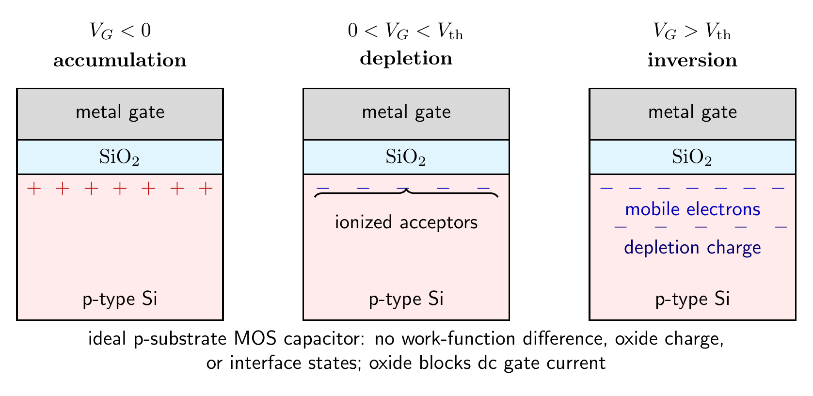
The editable source is mos-capacitor.tex.
A real structure has a work-function difference $\phi_{ms}$ and may contain fixed oxide charge, mobile ionic charge, oxide traps, and interface traps. If a bias-independent effective oxide sheet charge $Q_{ox}$ is used, the flat-band voltage is
\[\boxed{V_{FB}=\phi_{ms}-\frac{Q_{ox}}{C_{ox}}}.\]Here $\phi_{ms}$ is expressed in volts and $Q_{ox}$ in $\mathrm{C\,m^{-2}}$. Interface-trap charge can depend on surface potential and cannot always be represented by a constant $Q_{ox}$.
Let $\psi_s$ be surface potential relative to the neutral bulk and $Q_s$ the signed semiconductor sheet charge. The electrostatic balance is
\[\boxed{V_G=V_{FB}+\psi_s-\frac{Q_s}{C_{ox}}}.\]For a uniformly doped p substrate under depletion,
\[Q_s\simeq Q_d=-\sqrt{2q\varepsilon_sN_A\psi_s}.\]Define the positive bulk Fermi potential
\[\phi_F=V_T\ln\!\left(\frac{N_A}{n_i}\right).\]Strong inversion is conventionally set at $\psi_s=2\phi_F$. With zero substrate-source bias and the depletion approximation, the n-channel threshold voltage is
\[\boxed{V_{\rm th}=V_{FB}+2\phi_F +\frac{\sqrt{4q\varepsilon_sN_A\phi_F}}{C_{ox}}}.\]Every term is in volts. This expression omits body bias, polysilicon depletion, quantum confinement, and short-channel effects.
The small-signal gate capacitance is $C_{ox}$ per unit area in accumulation. In depletion, the oxide and depletion capacitances are in series,
\[C_G=\frac{C_{ox}C_d}{C_{ox}+C_d}<C_{ox}.\]In strong inversion, a low-frequency signal allows minority carriers to follow and $C_G$ returns toward $C_{ox}$; at high frequency their response is too slow, so the capacitance remains near its minimum value. Interface states and mobile or trapped oxide charge stretch or shift these ideal curves.
Enhancement nMOS operation
Two n$^+$ regions form source and drain in the p substrate. For $V_{GS}>V_{\rm th}$, the inverted surface connects them. Let
\[K=\mu_nC_{ox}\frac WL,\]where $\mu_n$ is channel mobility, $W/L$ is dimensionless, and $K$ has units $\mathrm{A\,V^{-2}}$.
At position $x$ along a gradual channel, let $V(x)$ rise from $0$ at the source to $V_{DS}$ at the drain. The inversion-charge magnitude per unit area is
\[-Q_n(x)=C_{ox}\bigl[V_{GS}-V_{\rm th}-V(x)\bigr].\]The drift-current magnitude $I_D=-W\mu_nQ_n\,dV/dx$ is constant along the channel. Integrating from $x=0$ to $L$ gives
\[I_D=\mu_nC_{ox}\frac WL \int_0^{V_{DS}}\!\bigl(V_{GS}-V_{\rm th}-V\bigr)\,dV =K\left[(V_{GS}-V_{\rm th})V_{DS}-\frac{V_{DS}^2}{2}\right].\]This derivation requires a long channel, constant mobility, negligible source/drain series resistance, and $0\le V_{DS}\le V_{GS}-V_{\rm th}$. The ideal long-channel output characteristic is
\[I_D= \begin{cases} 0,&V_{GS}\le V_{\rm th},\\[4pt] K\!\left[(V_{GS}-V_{\rm th})V_{DS}-\dfrac{V_{DS}^2}{2}\right], &V_{GS}>V_{\rm th},\ 0\le V_{DS}<V_{GS}-V_{\rm th},\\[8pt] \dfrac K2(V_{GS}-V_{\rm th})^2, &V_{GS}>V_{\rm th},\ V_{DS}\ge V_{GS}-V_{\rm th}. \end{cases}\]The second line is the linear or triode region. Saturation begins when the channel pinches off at the drain, $V_{DS}=V_{GS}-V_{\rm th}$. As in a JFET, pinch-off does not mean zero current.
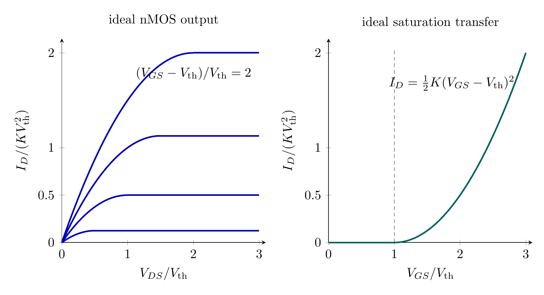
The editable source is mosfet-characteristics.tex.
At fixed saturation $V_{DS}$, the transfer characteristic is quadratic above threshold. A real MOSFET has subthreshold current below $V_{\rm th}$ and a finite saturation slope. The common channel-length-modulation approximation is
\[I_D\simeq\frac K2(V_{GS}-V_{\rm th})^2(1+\lambda V_{DS}),\]where $\lambda$ has units $\mathrm{V^{-1}}$. Mobility reduction, series resistance, and heating cause further departures. A pMOS device uses a p-channel and reversed voltage and current polarities; its magnitude equations follow after replacing overdrive by $V_{SG}-\lvert V_{\rm th}\rvert$.
Solved Problems
1. Oxide capacitance and flat-band shift
A silicon dioxide layer has $\varepsilon_{ox}=3.9\varepsilon_0$, $t_{ox}=10.0\,\mathrm{nm}$, $\varepsilon_0=8.854\times10^{-12}\,\mathrm{F\,m^{-1}}$, $\phi_{ms}=-0.100\,\mathrm V$, and an effective positive oxide charge $Q_{ox}=2.00\times10^{-4}\,\mathrm{C\,m^{-2}}$.
\[C_{ox}=\frac{3.9(8.854\times10^{-12})}{10.0\times10^{-9}} =3.453\times10^{-3}\,\mathrm{F\,m^{-2}}.\]Equivalently, $C_{ox}=3.453\,\mathrm{fF\,\mu m^{-2}}$. The flat-band voltage is
\[V_{FB}=-0.100-\frac{2.00\times10^{-4}}{3.453\times10^{-3}} =-0.1579\,\mathrm V.\]Positive oxide charge therefore shifts the required gate voltage in the negative direction, consistent with the minus sign in $V_{FB}$.
2. Threshold voltage of an idealized nMOS structure
At $300\,\mathrm K$, take $V_T=0.02585\,\mathrm V$, $N_A=1.00\times10^{22}\,\mathrm{m^{-3}}$, $n_i=1.00\times10^{16}\,\mathrm{m^{-3}}$, $\varepsilon_s=11.7\varepsilon_0$, $C_{ox}=3.453\times10^{-3}\,\mathrm{F\,m^{-2}}$, and $V_{FB}=-0.200\,\mathrm V$.
First,
\[\phi_F=V_T\ln\!\left(\frac{N_A}{n_i}\right) =(0.02585)\ln(10^6)=0.3571\,\mathrm V.\]The depletion-charge contribution is
\[\frac{\sqrt{4q\varepsilon_sN_A\phi_F}}{C_{ox}}=0.1410\,\mathrm V.\]Hence
\[V_{\rm th}=-0.200+2(0.3571)+0.1410=0.6553\,\mathrm V.\]Every term is a voltage; the positive result means a positive gate bias is needed to create strong inversion.
3. Triode and saturation currents from geometry
Let $\mu_n=0.0500\,\mathrm{m^2\,V^{-1}\,s^{-1}}$, $C_{ox}=3.00\,\mathrm{mF\,m^{-2}}$, $W/L=10.0$, $V_{\rm th}=1.00\,\mathrm V$, and $V_{GS}=3.50\,\mathrm V$. Then
\[K=\mu_nC_{ox}\frac WL=1.50\,\mathrm{mA\,V^{-2}}.\]For $V_{DS}=1.00\,\mathrm V<2.50\,\mathrm V$,
\[I_D=1.50\left[(2.50)(1.00)-\frac{1.00^2}{2}\right]=3.00\,\mathrm{mA}.\]At $V_{DS}\ge2.50\,\mathrm V$,
\[I_{D,sat}=\frac{1.50}{2}(2.50)^2=4.688\,\mathrm{mA}.\]Substituting $V_{DS}=2.50\,\mathrm V$ into the triode expression also gives $4.688\,\mathrm{mA}$, checking current continuity at the boundary.
Descriptive Questions
- Describe accumulation, depletion, and inversion in an ideal MOS capacitor on a p-type substrate.
- Explain how work-function difference, oxide charge, and interface states distinguish a real MOS capacitor from an ideal one.
- Derive the threshold-voltage expression from gate-voltage balance at $\psi_s=2\phi_F$.
- Derive the long-channel nMOS triode and saturation laws and state the assumptions under which they apply.
Numerical Problems
-
A high-frequency MOS measurement gives $C_{min}=1.20\,\mathrm{mF\,m^{-2}}$ while $C_{ox}=3.00\,\mathrm{mF\,m^{-2}}$. Treating $C_{min}$ as the series combination of $C_{ox}$ and the depletion capacitance $C_d$, find $C_d$ and the maximum depletion width for $\varepsilon_s=1.04\times10^{-10}\,\mathrm{F\,m^{-1}}$.
Final answer: $C_d=[1/C_{min}-1/C_{ox}]^{-1}=2.00\,\mathrm{mF\,m^{-2}}$ and $x_{d,max}=\varepsilon_s/C_d=52.0\,\mathrm{nm}$.
-
A MOS capacitor has $\phi_{ms}=-0.100\,\mathrm V$, $C_{ox}=4.00\,\mathrm{mF\,m^{-2}}$, and measured $V_{FB}=-0.250\,\mathrm V$. Infer the effective oxide-charge density and its sign.
Final answer: $Q_{ox}=C_{ox}(\phi_{ms}-V_{FB})=+6.00\times10^{-4}\,\mathrm{C\,m^{-2}}$; the charge is positive.
-
An nMOS capacitor has measured $V_{\rm th}=0.800\,\mathrm V$, $V_{FB}=-0.100\,\mathrm V$, $\phi_F=0.300\,\mathrm V$, $C_{ox}=2.50\,\mathrm{mF\,m^{-2}}$, and $N_A=2.00\times10^{22}\,\mathrm{m^{-3}}$. Using $q=1.60\times10^{-19}\,\mathrm C$, extract the maximum depletion-charge magnitude and depletion width.
Final answer: $\lvert Q_{d,max}\rvert=C_{ox}(V_{\rm th}-V_{FB}-2\phi_F)=7.50\times10^{-4}\,\mathrm{C\,m^{-2}}$ and $x_{d,max}=\lvert Q_{d,max}\rvert/(qN_A)=0.2344\,\mu\mathrm m$.
-
An nMOS channel has $C_{ox}=2.00\,\mathrm{mF\,m^{-2}}$, $W=20.0\,\mu\mathrm m$, $L=2.00\,\mu\mathrm m$, $V_{GS}=3.00\,\mathrm V$, $V_{\rm th}=1.00\,\mathrm V$, and $V_{DS}=1.00\,\mathrm V$. Assuming $V(x)$ varies linearly in the triode region, find the inversion-charge density at source and drain and the total mobile channel charge.
Final answer: $Q_n(0)=-4.00\times10^{-3}\,\mathrm{C\,m^{-2}}$, $Q_n(L)=-2.00\times10^{-3}\,\mathrm{C\,m^{-2}}$, and $Q_{ch}=-WLC_{ox}[V_{GS}-V_{\rm th}-V_{DS}/2]=-1.20\times10^{-13}\,\mathrm C$.
-
A rectangular MOS gate has $W=100\,\mu\mathrm m$, $L=10.0\,\mu\mathrm m$, and $C_{ox}=2.50\,\mathrm{mF\,m^{-2}}$. Neglect fringing and find the gate capacitance, charge magnitude at $V_G=3.30\,\mathrm V$, and stored electrostatic energy.
Final answer: $C_G=C_{ox}WL=2.50\,\mathrm{pF}$, $Q_G=C_GV_G=8.25\,\mathrm{pC}$, and $U_G=C_GV_G^2/2=13.61\,\mathrm{pJ}$.
The electrostatic identities, channel integration, boundary continuity, and all numerical results are reproducible in mos-capacitor-mosfet-check.mac; every printed residual is zero.


Discussion