

26 Jun 2025
Junction Bias, Current, Resistance, and Capacitance
Forward and reverse bias, diode current mechanisms, V-I characteristic, small-signal resistance, and junction capacitance.
Define the applied junction voltage by
\[V=V_p-V_n.\]Forward bias means $V>0$: the p terminal is at the higher potential, so the barrier is reduced from $V_{bi}$ to $V_{bi}-V$. Reverse bias means $V<0$ and increases the barrier to $V_{bi}+\lvert V\rvert$. In the depletion approximation,
\[\boxed{W(V)=\sqrt{\frac{2\varepsilon_s}{q} \left(\frac1{N_A}+\frac1{N_D}\right)(V_{bi}-V)}}.\]This expression requires $V<V_{bi}$ and fails in strong forward injection or breakdown.
Current-flow mechanism
Forward bias injects electrons from n into p and holes from p into n. At the depletion edges, the ideal low-injection boundary concentrations are
\[n_p(0)=n_{p0}e^{V/V_T}, \qquad p_n(0)=p_{n0}e^{V/V_T},\]where $n_{p0}=n_i^2/N_A$ and $p_{n0}=n_i^2/N_D$. The injected minority carriers diffuse through the neutral regions and recombine. For long quasi-neutral regions, $W_p\gg L_n$ and $W_n\gg L_p$, or equivalent remote-contact boundary conditions, solving their steady diffusion equations gives
\[\boxed{I=I_S\!\left(e^{V/(\eta V_T)}-1\right)}.\]For the ideal diffusion model, $\eta=1$ and
\[I_S=qA\left(\frac{D_n n_{p0}}{L_n}+\frac{D_p p_{n0}}{L_p}\right),\]where $A$ is junction area in $\mathrm{m^2}$, $D$ is diffusivity in $\mathrm{m^2\,s^{-1}}$, and $L$ is diffusion length in metres; $I_S$ is therefore in amperes. For finite neutral widths the corresponding terms acquire $\coth(W/L)$ factors. Depletion-region recombination commonly gives an effective $\eta$ approaching 2.
Under reverse bias with $\lvert V\rvert\gtrsim3\eta V_T$ but below breakdown, thermally generated minority carriers are swept across the depletion layer and $I\simeq-I_S$. At breakdown the reverse current is instead limited by the external circuit. At large forward current, series resistance and high-level injection cause departure from the exponential law.
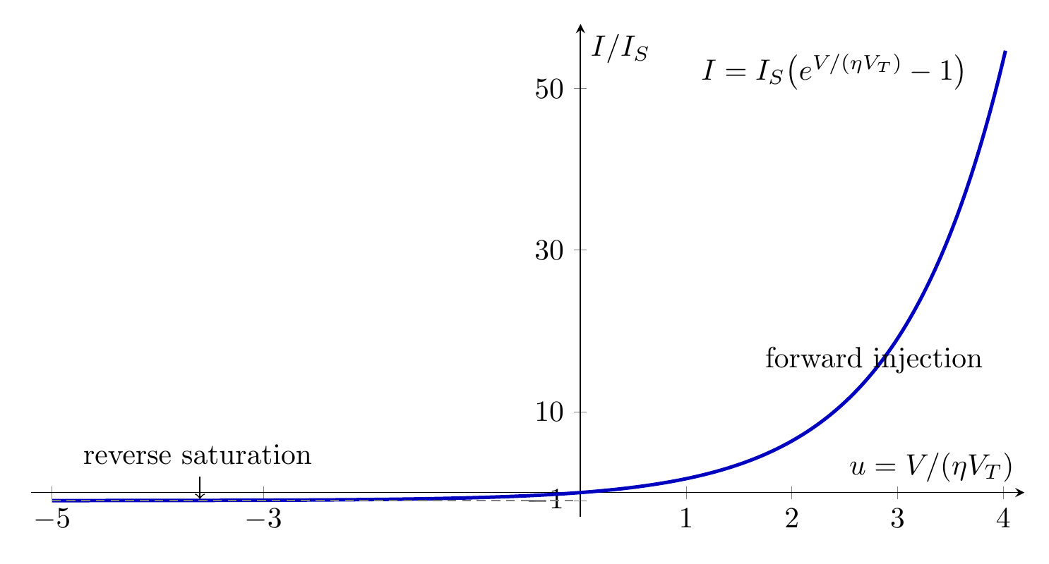
The editable source is diode-characteristic.tex.
Static and dynamic resistance
At a chosen operating point $(V,I)$, the dc or static resistance and the local small-signal resistance are different:
\[\boxed{R_{\rm dc}=\frac VI}, \qquad \boxed{r_d=\left(\frac{dI}{dV}\right)^{-1} =\frac{\eta V_T}{I+I_S} \simeq\frac{\eta V_T}{I}}.\]The last approximation requires strong forward bias, $I\gg I_S$. Both resistances have units ohms, but $r_d$ is the reciprocal slope at the operating point and governs only sufficiently small signal changes.
Junction and diffusion capacitance
The magnitude of depletion charge is $Q=qAN_Ax_p=qAN_Dx_n$. The depletion or transition capacitance is
\[\boxed{C_j=\left\lvert\frac{dQ}{dV}\right\rvert=\frac{\varepsilon_sA}{W} =\frac{C_{j0}}{\sqrt{1-V/V_{bi}}}}, \qquad C_{j0}=\frac{\varepsilon_sA}{W_0}.\]Thus reverse bias widens the layer and reduces $C_j$. This square-root law is for an abrupt junction; a graded junction has a different exponent. Under appreciable forward bias, stored injected charge adds a diffusion capacitance. If the stored charge is approximately $Q_s\simeq\tau_T I$,
\[\boxed{C_d=\frac{dQ_s}{dV}\simeq\frac{\tau_T I}{\eta V_T}},\]where $\tau_T$ is an effective carrier transit or storage time in seconds. The small-signal terminal capacitance is approximately $C_j+C_d$ before parasitic package capacitances are included.
Solved Problems
1. Forward current and the local diode resistance
A diode has $I_S=10.0\,\mathrm{nA}$, $\eta=1.50$, and $V_T=25.9\,\mathrm{mV}$. Find its current, static resistance, and dynamic resistance at $V=0.300\,\mathrm V$.
\[\frac{V}{\eta V_T}=\frac{0.300}{(1.50)(0.0259)}=7.722,\] \[I=10.0\,\mathrm{nA}\,[e^{7.722}-1]=22.56\,\mu\mathrm A.\]Thus
\[R_{dc}=\frac{0.300}{22.56\,\mu\mathrm A}=13.30\,\mathrm{k\Omega},\] \[r_d=\frac{(1.50)(0.0259)}{I+I_S}=1.721\,\mathrm{k\Omega}.\]The much smaller $r_d$ is the tangent resistance, not a contradiction: the exponential curve steepens as the bias increases. Substitution gives $r_d(dI/dV)=1$.
2. Reverse-bias depletion and forward-bias storage capacitance
An abrupt junction has $W_0=0.600\,\mu\mathrm m$, $C_{j0}=40.0\,\mathrm{pF}$, and $V_{bi}=0.720\,\mathrm V$. At $V=-5.00\,\mathrm V$,
\[W=W_0\sqrt{1-\frac{V}{V_{bi}}} =0.600\sqrt{1+\frac{5.00}{0.720}} =1.691\,\mu\mathrm m,\] \[C_j=\frac{40.0}{\sqrt{1+5.00/0.720}}=14.19\,\mathrm{pF}.\]Reverse bias therefore increases $W$ and decreases $C_j$, with $WC_j=W_0C_{j0}$ in this model. Separately, at forward current $I=2.00\,\mathrm{mA}$ with $\tau_T=2.00\,\mu\mathrm s$, $\eta=1.50$, and $V_T=25.9\,\mathrm{mV}$,
\[C_d\simeq\frac{\tau_TI}{\eta V_T}=0.10296\,\mu\mathrm F=103\,\mathrm{nF}.\]This much larger value reflects stored injected charge under forward bias, not depletion charge.
Descriptive Questions
- Explain how forward and reverse bias change the junction barrier and depletion width.
- Derive the Shockley diode equation from minority-carrier boundary conditions and state the long-neutral-region assumption.
- Distinguish static and dynamic diode resistance and specify the signal range for which $r_d$ is useful.
- Compare depletion and diffusion capacitance in origin, bias dependence, and dominant operating regime.
Numerical Problems
-
For a long-base diode use $A=0.500\,\mathrm{mm^2}$, $q=1.60\times10^{-19}\,\mathrm C$, $n_i=1.00\times10^{16}\,\mathrm{m^{-3}}$, $N_A=2.00\times10^{22}\,\mathrm{m^{-3}}$, $N_D=5.00\times10^{21}\,\mathrm{m^{-3}}$, $D_n=3.00\times10^{-3}\,\mathrm{m^2\,s^{-1}}$, $D_p=1.00\times10^{-3}\,\mathrm{m^2\,s^{-1}}$, $L_n=30.0\,\mu\mathrm m$, and $L_p=20.0\,\mu\mathrm m$. Find the electron and hole contributions to $I_S$ and their sum.
Final answer: $n_{p0}=5.00\times10^9\,\mathrm{m^{-3}}$ and $p_{n0}=2.00\times10^{10}\,\mathrm{m^{-3}}$. Therefore $I_{S,n}=0.0400\,\mathrm{pA}$, $I_{S,p}=0.0800\,\mathrm{pA}$, and $I_S=0.120\,\mathrm{pA}=1.20\times10^{-13}\,\mathrm A$.
-
A diode with $I_S=5.00\,\mathrm{nA}$ and $\eta=2$ is biased at $V=-0.200\,\mathrm V$ at $300\,\mathrm K$. Find its current.
Final answer: $I=5.00\,\mathrm{nA}[e^{-0.200/(2\times0.0259)}-1]=-4.895\,\mathrm{nA}$, close to the reverse-saturation value $-I_S$.
-
At a strong-forward-bias point where $I\gg I_S$, a curve tracer measures $I=1.00\,\mathrm{mA}$ and differential conductance $g_d=dI/dV=25.0\,\mathrm{mS}$. With $V_T=25.0\,\mathrm{mV}$, infer $r_d$ and $\eta$. What current amplitude is produced by a sufficiently small $2.00\,\mathrm{mV}$ voltage amplitude?
Final answer: $r_d=1/g_d=40.0\,\Omega$ and $\eta=I/(g_dV_T)=1.60$. The small-signal current amplitude is $\Delta i=g_d\Delta v=50.0\,\mu\mathrm A$.
-
An abrupt junction gives $C_j=30.0\,\mathrm{pF}$ at $V=-2.25\,\mathrm V$ and $20.0\,\mathrm{pF}$ at $V=-6.00\,\mathrm V$. Use the abrupt-junction law to infer $V_{bi}$ and $C_{j0}$, then predict $C_j$ at $V=-11.25\,\mathrm V$.
Final answer: Squaring the capacitance ratio gives $9/4=(V_{bi}+6)/(V_{bi}+9/4)$, hence $V_{bi}=3/4=0.750\,\mathrm V$. Either measurement gives $C_{j0}=60.0\,\mathrm{pF}$, and $C_j(-11.25\,\mathrm V)=60/\sqrt{16}=15.0\,\mathrm{pF}$.
The exponential law, resistance derivative, capacitance identities, and all numerical values are reproducible in pn-junction-bias-check.mac; every printed residual is zero.


Discussion