

25 Jun 2025
p-n Junction Formation, Depletion Region, and Barrier
Diffusion, space charge, built-in potential, electric field, and depletion width of an abrupt p-n junction.
Consider a one-dimensional abrupt homojunction with uniformly doped p material at $x<0$ and n material at $x>0$. Let $q=1.602\times10^{-19}\,\mathrm C$ denote the positive elementary-charge magnitude. The depletion approximation used below assumes complete dopant ionization and neglects mobile carriers inside the depleted layer.
Formation of the space-charge region
Before contact, the n side contains many electrons and the p side many holes. After contact, electrons diffuse from n to p and holes diffuse from p to n. Recombination near the interface leaves fixed ionized acceptors $-qN_A$ on the p side and fixed ionized donors $+qN_D$ on the n side. Their electric field points from the positive donor charge toward the negative acceptor charge, namely from n to p.
If the depletion edges are $-x_p$ and $x_n$, the charge density is
\[\rho(x)= \begin{cases} -qN_A,&-x_p<x<0,\\ +qN_D,&0<x<x_n,\\ 0,&\text{elsewhere}. \end{cases}\]Charge neutrality of the depletion layer requires
\[\boxed{N_Ax_p=N_Dx_n}.\]Poisson’s equation and the electric-field sign convention are
\[\frac{dE}{dx}=\frac{\rho}{\varepsilon_s}, \qquad E=-\frac{d\phi}{dx},\]where $\varepsilon_s$ is the semiconductor permittivity in $\mathrm{F\,m^{-1}}$. With $E(-x_p)=E(x_n)=0$,
\[E(x)= \begin{cases} -\dfrac{qN_A}{\varepsilon_s}(x+x_p),&-x_p\le x\le0,\\[6pt] \dfrac{qN_D}{\varepsilon_s}(x-x_n),&0\le x\le x_n. \end{cases}\]Thus $E<0$ throughout the depletion region: it opposes further majority-carrier diffusion. Equilibrium is reached when drift and diffusion currents cancel separately for electrons and holes.
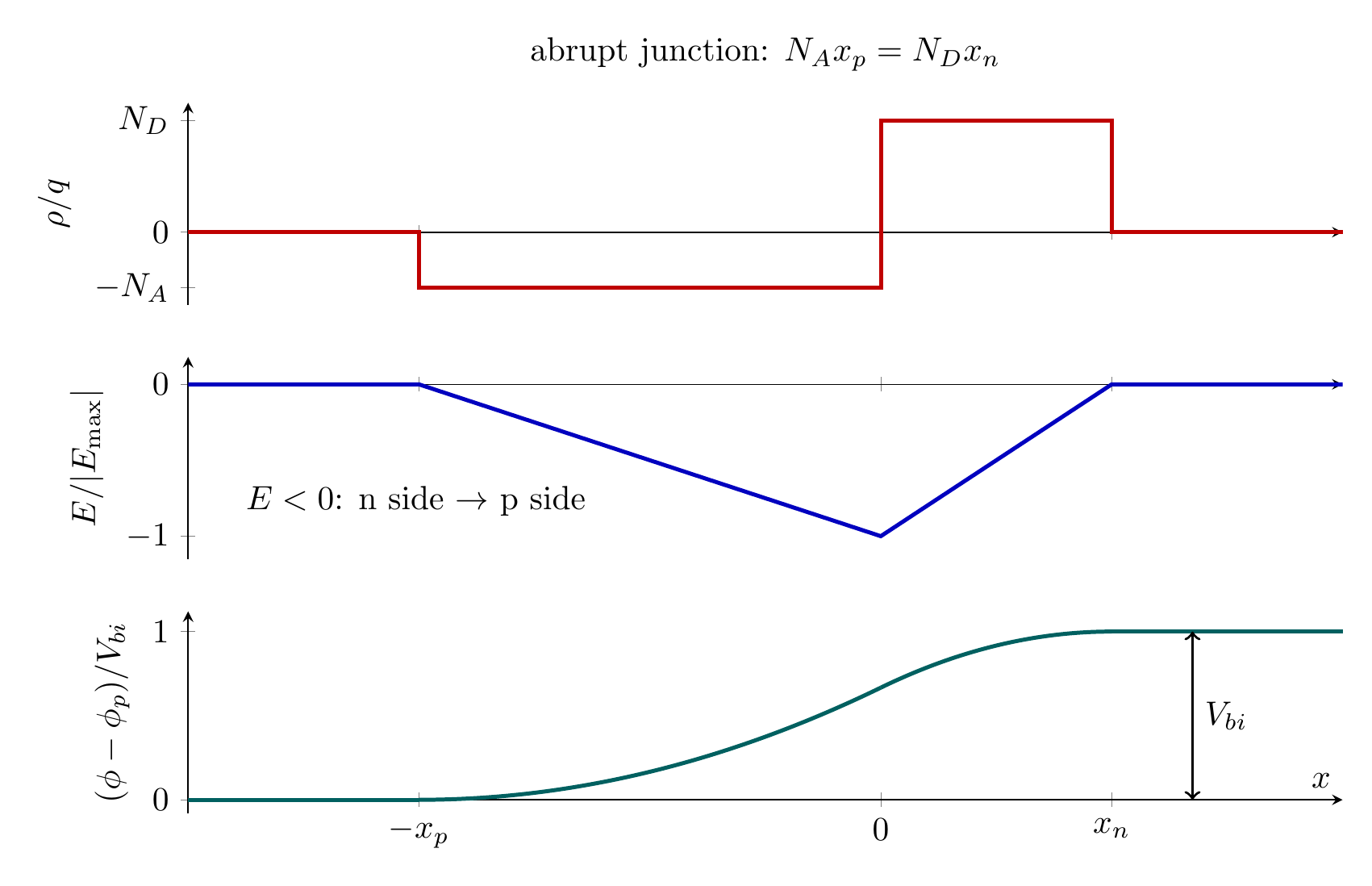
The editable source is pn-junction-depletion.tex.
Built-in potential and depletion width
At thermal equilibrium the Fermi level is constant. For non-degenerate material with $n_n\simeq N_D$ and $p_p\simeq N_A$, the electrostatic potential difference is
\[\boxed{V_{bi}=\phi_n-\phi_p =V_T\ln\!\left(\frac{N_AN_D}{n_i^2}\right)}, \qquad V_T=\frac{k_BT}{q}.\]$V_T$ is the thermal voltage, equal to about $25.9\,\mathrm{mV}$ at $300\,\mathrm K$. The formula assumes $N_AN_D>n_i^2$, complete ionization, and Maxwell-Boltzmann statistics. Integrating $-E=d\phi/dx$ gives
\[V_{bi}=\frac{q}{2\varepsilon_s} \left(N_Ax_p^2+N_Dx_n^2\right).\]Writing $W_0=x_p+x_n$,
\[\boxed{W_0=\sqrt{\frac{2\varepsilon_sV_{bi}}q \left(\frac1{N_A}+\frac1{N_D}\right)}},\] \[x_p=\frac{N_D}{N_A+N_D}W_0, \qquad x_n=\frac{N_A}{N_A+N_D}W_0.\]The depletion region extends farther into the more lightly doped side. The peak field magnitude is
\[\lvert E_{\max}\rvert=\frac{qN_Ax_p}{\varepsilon_s} =\frac{qN_Dx_n}{\varepsilon_s} =\frac{2V_{bi}}{W_0},\]with units $\mathrm{V\,m^{-1}}$. Since an electron’s band energy changes as $-q\phi$, the conduction and valence band edges fall by $qV_{bi}$ from the p side to the n side; this band bending is the equilibrium barrier to majority-carrier diffusion.
Solved Problems
1. Built-in potential and asymmetric depletion widths
For silicon at $300\,\mathrm K$, take $N_A=1.00\times10^{23}\,\mathrm{m^{-3}}$, $N_D=1.00\times10^{22}\,\mathrm{m^{-3}}$, $n_i=1.00\times10^{16}\,\mathrm{m^{-3}}$, $V_T=0.02585\,\mathrm V$, and $\varepsilon_s=11.7\varepsilon_0$ with $\varepsilon_0=8.854\times10^{-12}\,\mathrm{F\,m^{-1}}$.
The built-in potential is
\[V_{bi}=0.02585\ln\!\left(\frac{10^{23}10^{22}}{(10^{16})^2}\right) =0.7738\,\mathrm V.\]The total depletion width is
\[W_0=\sqrt{\frac{2(11.7\varepsilon_0)(0.7738)}{q} \left(\frac1{10^{23}}+\frac1{10^{22}}\right)} =3.318\times10^{-7}\,\mathrm m=0.3318\,\mu\mathrm m.\]Charge neutrality then gives
\[x_p=\frac{N_D}{N_A+N_D}W_0=0.03016\,\mu\mathrm m, \qquad x_n=0.3016\,\mu\mathrm m.\]The n side is ten times more lightly doped, so its depleted width is ten times larger. The independent check $N_Ax_p=N_Dx_n$ is exact before rounding.
2. Peak field from the triangular field profile
A symmetric abrupt silicon junction has $N_A=N_D=5.00\times10^{22}\,\mathrm{m^{-3}}$ and $V_{bi}=0.700\,\mathrm V$. With the same $\varepsilon_s$,
\[W_0=\sqrt{\frac{4\varepsilon_sV_{bi}}{qN}} =1.903\times10^{-7}\,\mathrm m.\]Symmetry gives $x_p=x_n=W_0/2=0.09515\,\mu\mathrm m$. Because the potential is the area under $-E(x)$ and the field profile is triangular,
\[V_{bi}=\frac12W_0\lvert E_{\max}\rvert,\]so
\[\lvert E_{\max}\rvert=\frac{2V_{bi}}{W_0} =7.357\times10^6\,\mathrm{V\,m^{-1}}.\]Substitution into $qNx_n/\varepsilon_s$ gives the same magnitude; the signed field itself is negative because it points from n to p.
Descriptive Questions
- Explain how carrier diffusion creates the space-charge region and built-in electric field of a p-n junction.
- Derive the piecewise electric field from Poisson’s equation under the depletion approximation.
- Derive the built-in-potential and total-depletion-width expressions, stating all statistical and electrostatic assumptions.
- Explain why the depletion layer extends farther into the more lightly doped side and relate this to charge neutrality.
Numerical Problems
-
Microscopy of an abrupt junction gives depletion extents $x_p=0.120\,\mu\mathrm m$ and $x_n=0.480\,\mu\mathrm m$. If $N_D=2.50\times10^{21}\,\mathrm{m^{-3}}$, find $N_A$, the uncovered-ion sheet density on either side, and the magnitude of each fixed sheet charge. Use $q=1.602\times10^{-19}\,\mathrm C$.
Final answer: Charge neutrality gives $N_A=N_Dx_n/x_p=1.00\times10^{22}\,\mathrm{m^{-3}}$. Hence $N_s=N_Ax_p=N_Dx_n=1.20\times10^{15}\,\mathrm{m^{-2}}$ and $\lvert\sigma\rvert=qN_s=1.9224\times10^{-4}\,\mathrm{C\,m^{-2}}$; the p-side sheet is negative and the n-side sheet positive.
-
For an abrupt junction take $N_A=2.00\times10^{22}\,\mathrm{m^{-3}}$, $N_D=4.00\times10^{22}\,\mathrm{m^{-3}}$, $x_p=0.300\,\mu\mathrm m$, $x_n=0.150\,\mu\mathrm m$, and $\varepsilon_s=1.00\times10^{-10}\,\mathrm{F\,m^{-1}}$. Evaluate the signed field at $x=-0.100\,\mu\mathrm m$ and $x=+0.050\,\mu\mathrm m$, and verify that the field is continuous at $x=0$.
Final answer: The p-side and n-side formulae both give $E=-6.408\times10^6\,\mathrm{V\,m^{-1}}$ at the stated points. At the interface they independently give $E(0)=-9.612\times10^6\,\mathrm{V\,m^{-1}}$, so the field is continuous and directed toward p.
-
At fixed temperature, $N_A$, and $n_i$, a donor implant increases $N_D$ by a factor of $16$. If $V_T=0.0250\,\mathrm V$ and the original built-in potential was $0.620\,\mathrm V$, find the barrier increase and the new built-in potential.
Final answer: $\Delta V_{bi}=V_T\ln16=(\ln2)/10\,\mathrm V=0.06931\,\mathrm V$, so $V_{bi,\mathrm{new}}=31/50+(\ln2)/10=0.6893\,\mathrm V$.
-
An asymmetric junction has $x_p=0.150\,\mu\mathrm m$, $x_n=0.450\,\mu\mathrm m$, and $V_{bi}=0.840\,\mathrm V$. Find the p-side and n-side contributions to the built-in potential, and hence the junction potential relative to the neutral p side.
Final answer: Neutrality makes $V_p/V_n=x_p/x_n=1/3$. Thus $V_p=V_{bi}x_p/(x_p+x_n)=0.210\,\mathrm V$ and $V_n=0.630\,\mathrm V$; the metallurgical junction is $0.210\,\mathrm V$ above the neutral p side.
The Poisson-law identities and all numerical results are reproducible in pn-junction-formation-check.mac; every printed residual is zero.


Discussion