

29 Jun 2025
Zener Breakdown and Voltage Regulation
Zener and avalanche mechanisms, reverse characteristic, and the shunt voltage-regulator operating limits.
A Zener diode is designed to operate safely in reverse breakdown. Let $V_Z>0$ denote the magnitude of its specified reverse voltage. Below the knee the reverse current is small; near $V_R=V_Z$, current rises sharply while the terminal voltage changes only slightly. The external circuit must limit current because breakdown itself does not.
Zener and avalanche mechanisms
In a heavily doped junction the depletion layer is narrow and the electric field can become large at a relatively low reverse voltage. Electrons then tunnel quantum mechanically between valence- and conduction-band states. This is Zener breakdown and normally has a negative temperature coefficient of $V_Z$.
In a more lightly doped, wider junction, carriers gain kinetic energy from the field and create new electron-hole pairs by impact ionization. Repeated multiplication produces avalanche breakdown, normally with a positive temperature coefficient. Both mechanisms can contribute near approximately $5$–$6\,\mathrm V$; the distinction is physical, not a different circuit symbol.
The incremental resistance in breakdown is
\[\boxed{r_Z=\frac{dV_Z}{dI_Z}},\]measured in ohms. It is small but not zero, so a real Zener voltage varies with current and temperature.
Shunt regulator
The diode is reverse connected across the load and fed through a series resistance $R_s$.
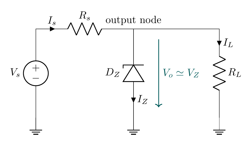
The editable source is zener-regulator.tex.
With $V_o\simeq V_Z$, Kirchhoff’s laws give
\[I_s=\frac{V_s-V_Z}{R_s}, \qquad I_L=\frac{V_Z}{R_L}, \qquad \boxed{I_Z=I_s-I_L}.\]Regulation requires
\[I_{Z,\min}\le I_Z\le I_{Z,\max},\]where the lower bound keeps the diode beyond its knee and the upper bound satisfies both current and power ratings:
\[P_Z=V_ZI_Z\le P_{Z,\max}.\]The worst-case input limits are therefore
\[V_{s,\min}\ge V_Z+R_s(I_{L,\max}+I_{Z,\min}),\] \[V_{s,\max}\le V_Z+R_s(I_{L,\min}+I_{Z,\max}).\]If either inequality is violated, the diode leaves regulation or overheats. In the small-signal model the Zener is $r_Z$, so
\[\frac{\Delta V_o}{\Delta V_s} =\frac{r_Z\parallel R_L}{R_s+(r_Z\parallel R_L)}.\]Good line regulation requires $r_Z\parallel R_L\ll R_s$, while load regulation also requires enough current margin for the change in $I_L$.
Solved Problems
1. Check current and power margins
A shunt regulator has $V_s=12.0\,\mathrm V$, $R_s=330\,\Omega$, $V_Z=5.10\,\mathrm V$, and $R_L=1.00\,\mathrm{k\Omega}$.
\[I_s=\frac{12.0-5.10}{330}=20.91\,\mathrm{mA}, \qquad I_L=\frac{5.10}{1.00\,\mathrm{k\Omega}}=5.10\,\mathrm{mA}.\]Node-current balance gives
\[I_Z=I_s-I_L=15.81\,\mathrm{mA}.\]The Zener dissipation is
\[P_Z=(5.10)(15.81\,\mathrm{mA})=80.6\,\mathrm{mW}.\]Thus a $0.50\,\mathrm W$ diode has ample power margin, provided $15.81\,\mathrm{mA}$ also exceeds its specified knee current. The check $20.91=5.10+15.81\,\mathrm{mA}$ fixes the current signs.
2. Design a resistor for input and load extremes
A $6.00\,\mathrm V$, $0.50\,\mathrm W$ Zener must regulate while $9.00\le V_s\le15.0\,\mathrm V$ and $0\le I_L\le20.0\,\mathrm{mA}$. Require $I_{Z,\min}=5.00\,\mathrm{mA}$.
At minimum input and maximum load,
\[R_s\le\frac{9.00-6.00}{20.0\,\mathrm{mA}+5.00\,\mathrm{mA}} =120\,\Omega.\]The power rating gives $I_{Z,\max}=0.50/6.00=83.33\,\mathrm{mA}$. At maximum input and zero load,
\[R_s\ge\frac{15.0-6.00}{83.33\,\mathrm{mA}}=108\,\Omega.\]Choose $R_s=110\,\Omega$. Then the two limiting currents are
\[I_Z(9.00\,\mathrm V,20.0\,\mathrm{mA}) =\frac{3.00}{110}-20.0\,\mathrm{mA} =7.27\,\mathrm{mA},\] \[I_Z(15.0\,\mathrm V,0) =\frac{9.00}{110}=81.82\,\mathrm{mA},\]so $P_Z=0.491\,\mathrm W<0.50\,\mathrm W$. Both the knee and power constraints are satisfied, though the upper margin is deliberately small.
Descriptive Questions
- Compare Zener tunnelling and avalanche multiplication, including doping, depletion width, and temperature coefficient.
- Explain the reverse characteristic and the physical meaning of knee current and dynamic resistance.
- Derive the current and power inequalities for a loaded Zener shunt regulator.
- Explain how $R_s$, $r_Z$, and $R_L$ determine small-signal line and load regulation.
Numerical Problems
-
A nominal $5.10\,\mathrm V$ Zener is connected to an $8.00\,\mathrm V$ source through $R_s=330\,\Omega$, with $R_L=470\,\Omega$ across the output. Test the assumption that the diode is regulating; if it is not, find the actual output voltage using the off-state model.
Final answer: Assuming $V_o=5.10\,\mathrm V$ gives $I_s=8.788\,\mathrm{mA}$, $I_L=10.85\,\mathrm{mA}$, and the impossible result $I_Z=-2.063\,\mathrm{mA}$. The Zener is therefore off, so $V_o=8.00[470/(330+470)]=4.70\,\mathrm V$ and $I_L=10.00\,\mathrm{mA}$.
-
A small-signal test of a Zener regulator with $R_s=500\,\Omega$ and $R_L=1.00\,\mathrm{k\Omega}$ gives $\Delta V_o=50.0\,\mathrm{mV}$ for $\Delta V_s=2.55\,\mathrm V$. Infer the Zener dynamic resistance $r_Z$.
Final answer: The measured gain is $A_v=0.0500/2.55=1/51$. Hence $r_Z\parallel R_L=A_vR_s/(1-A_v)=10.0\,\Omega$, which gives $r_Z=10.0(1000)/(1000-10.0)=10.10\,\Omega$.
-
Junction A breaks down at $4.80\,\mathrm V$ across an $80.0\,\mathrm{nm}$ depletion layer, while junction B breaks down at $12.0\,\mathrm V$ across $0.800\,\mu\mathrm m$. Estimate each average breakdown field and identify which junction is more consistent with Zener tunnelling and which with avalanche multiplication.
Final answer: $E_A\simeq4.80/(80.0\,\mathrm{nm})=6.00\times10^7\,\mathrm{V\,m^{-1}}$ and $E_B\simeq12.0/(0.800\,\mu\mathrm m)=1.50\times10^7\,\mathrm{V\,m^{-1}}$. Junction A has four times the average field in a much narrower layer and is more consistent with Zener tunnelling; junction B is more consistent with avalanche multiplication.
-
A regulating Zener has sufficient knee and power margin, $R_s=470\,\Omega$, and dynamic resistance $r_Z=10.0\,\Omega$. Treat the input source as ac-stiff. If the load current suddenly increases by $2.00\,\mathrm{mA}$, find the small-signal output resistance, the output-voltage change, and the new output from a nominal $5.60\,\mathrm V$.
Final answer: $R_{out}=R_s\parallel r_Z=9.792\,\Omega$, so $\Delta V_o=-R_{out}\Delta I_L=-19.58\,\mathrm{mV}$. The output falls to approximately $5.580\,\mathrm V$.
The regulator inequalities, current balance, power checks, and all numerical values are reproducible in zener-regulator-check.mac; every printed residual is zero.


Discussion