

28 Jun 2025
Combinational and Sequential Circuits
Universal-gate realizations, SOP/POS networks, data selectors and converters, arithmetic circuits, comparators, serial addition, and TTL/CMOS logic.
A combinational circuit has outputs determined by the present input word. A sequential circuit also contains state, so its output can depend on earlier inputs. Propagation is physical rather than instantaneous: if an input transition occurs at $t_0$, a specified output becomes valid only after a propagation delay $t_{pd}$, measured in seconds and commonly quoted in nanoseconds.
Logic gates and XOR
For positive logic, the elementary two-input functions are
| $A$ | $B$ | AND $AB$ | OR $A+B$ | NAND $\overline{AB}$ | NOR $\overline{A+B}$ | XOR $A\oplus B$ |
|---|---|---|---|---|---|---|
| 0 | 0 | 0 | 0 | 1 | 1 | 0 |
| 0 | 1 | 0 | 1 | 1 | 0 | 1 |
| 1 | 0 | 0 | 1 | 1 | 0 | 1 |
| 1 | 1 | 1 | 1 | 0 | 0 | 0 |
NOT is the one-input function $Y=\overline A$. XOR is 1 precisely when the inputs differ. Starting from that condition,
\[\begin{aligned} A\oplus B &=\overline AB+A\overline B\\ &=(A+B)(\overline A+\overline B), \end{aligned}\]where expansion of the second line gives $A\overline A+A\overline B+B\overline A+B\overline B=A\overline B+\overline AB$.
NAND and NOR as universal gates
A gate is universal if copies of that gate can generate NOT, AND, and OR, and hence any Boolean function.
For NAND, joining the inputs gives inversion:
\[\overline A=A\mathbin{\mathrm{NAND}}A.\]Inverting a NAND output gives AND,
\[AB=(A\mathbin{\mathrm{NAND}}B)\mathbin{\mathrm{NAND}}(A\mathbin{\mathrm{NAND}}B),\]and De Morgan gives OR:
\[A+B=(A\mathbin{\mathrm{NAND}}A)\mathbin{\mathrm{NAND}}(B\mathbin{\mathrm{NAND}}B).\]The dual construction uses only NOR:
\[\begin{aligned} \overline A&=A\mathbin{\mathrm{NOR}}A,\\ A+B&=(A\mathbin{\mathrm{NOR}}B)\mathbin{\mathrm{NOR}}(A\mathbin{\mathrm{NOR}}B),\\ AB&=(A\mathbin{\mathrm{NOR}}A)\mathbin{\mathrm{NOR}}(B\mathbin{\mathrm{NOR}}B). \end{aligned}\]SOP and POS realization
An SOP expression uses one AND gate per product term and an OR gate to combine those terms. For
\[F=\overline AC+AB,\]the direct network is a two-level AND-OR circuit. It can be changed to a NAND-NAND network without changing the function:
\[F=\overline{\overline{\overline AC+AB}} =\overline{\,\overline{\overline AC}\;\overline{AB}\,}.\]The inner NAND gates produce complemented products and the final NAND performs their OR by De Morgan’s law.
A POS expression uses one OR gate per sum term and an AND gate at the output. For example,
\[G=(A+\overline B)(C+D) =\overline{\,\overline{A+\overline B}+\overline{C+D}\,},\]which is a NOR-NOR realization. Complemented input literals require an input inverter unless both polarities are already available.
Decoders and encoders
An $n$-to-$2^n$ decoder asserts one minterm selected by the $n$-bit input. A 2-to-4 active-high decoder has
\[\begin{aligned} D_0&=\overline A_1\,\overline A_0,& D_1&=\overline A_1A_0,\\ D_2&=A_1\overline A_0,& D_3&=A_1A_0. \end{aligned}\]Exactly one $D_k$ is 1 for each input word. Therefore a decoder can realize
\[F(A_1,A_0)=\Sigma m(k_1,k_2,\ldots)\]by ORing the corresponding decoded outputs.
An encoder performs the reverse operation when its inputs are one-hot. For inputs $D_0,D_1,D_2,D_3$, the encoded output is
\[A_1=D_2+D_3,\qquad A_0=D_1+D_3.\]If more than one $D_k$ is high, these equations do not identify a unique input; the one-hot condition is therefore part of the encoder specification.
Multiplexers and demultiplexers
A multiplexer selects one data input. For a 4-to-1 device,
\[\begin{aligned} Y={}&\overline S_1\overline S_0I_0 +\overline S_1S_0I_1\\ &+S_1\overline S_0I_2+S_1S_0I_3. \end{aligned}\]Only one select minterm is 1, so $Y=I_0,I_1,I_2,$ or $I_3$ for $S_1S_0=00,01,10,$ or $11$. A demultiplexer distributes one input $X$ to one selected output:
\[Y_0=X\overline S_1\overline S_0,\quad Y_1=X\overline S_1S_0,\quad Y_2=XS_1\overline S_0,\quad Y_3=XS_1S_0.\]Code conversion with gates and MSI circuits
A code converter is a combinational mapping. Its design begins with the valid input-code words, assigns every required output bit, treats invalid input words only as specified don’t-cares, and minimizes each output function.
For the decimal digit codes already defined in Unit I, let $B_3B_2B_1B_0$ be a valid 8421 BCD digit. The seven-bit ASCII digit has the form
\[(X_6X_5X_4X_3X_2X_1X_0)_{\rm ASCII} =(011B_3B_2B_1B_0)_2.\]Hence
\[X_6=0,\quad X_5=X_4=1,\quad (X_3X_2X_1X_0)=(B_3B_2B_1B_0).\]For example, BCD 5 is 0101, giving ASCII 0110101 $=53_{10}$, the code for the character 5. At gate level this converter needs constants and direct connections. In a general converter, a decoder produces input minterms and OR gates combine the minterms required by each output bit. A multiplexer can instead use the code bits as select inputs and store one output truth-table column on its data inputs. Decoders, encoders, multiplexers, and demultiplexers are MSI functions: each integrated circuit contains a complete medium-scale logic block rather than one elementary gate.
Half adder and full adder
A half adder adds two one-bit integers. Since the arithmetic value must satisfy
\[A+B=S+2C,\]its truth table gives
\[S=A\oplus B,\qquad C=AB.\]A full adder also accepts $C_{in}$. Use a first half adder to form
\[S_1=A\oplus B,\qquad C_1=AB,\]and a second to form
\[S=S_1\oplus C_{in},\qquad C_2=S_1C_{in}.\]The two partial carries cannot both arise from different numerical values requiring separate output bits; their OR is the outgoing carry:
\[\boxed{S=A\oplus B\oplus C_{in}},\] \[\boxed{C_{out}=AB+C_{in}(A\oplus B)=AB+AC_{in}+BC_{in}}.\]For all eight input rows,
\[A+B+C_{in}=S+2C_{out}.\]Serial adder and clock convention
A serial adder reuses one full adder for successive bit positions, starting at the least significant bit. During clock interval $i$ it computes
\[S_i=A_i\oplus B_i\oplus C_i,\qquad C_{i+1}=A_iB_i+C_i(A_i\oplus B_i),\]then stores $C_{i+1}$ for interval $i+1$. Thus it is sequential even though its full-adder core is combinational.
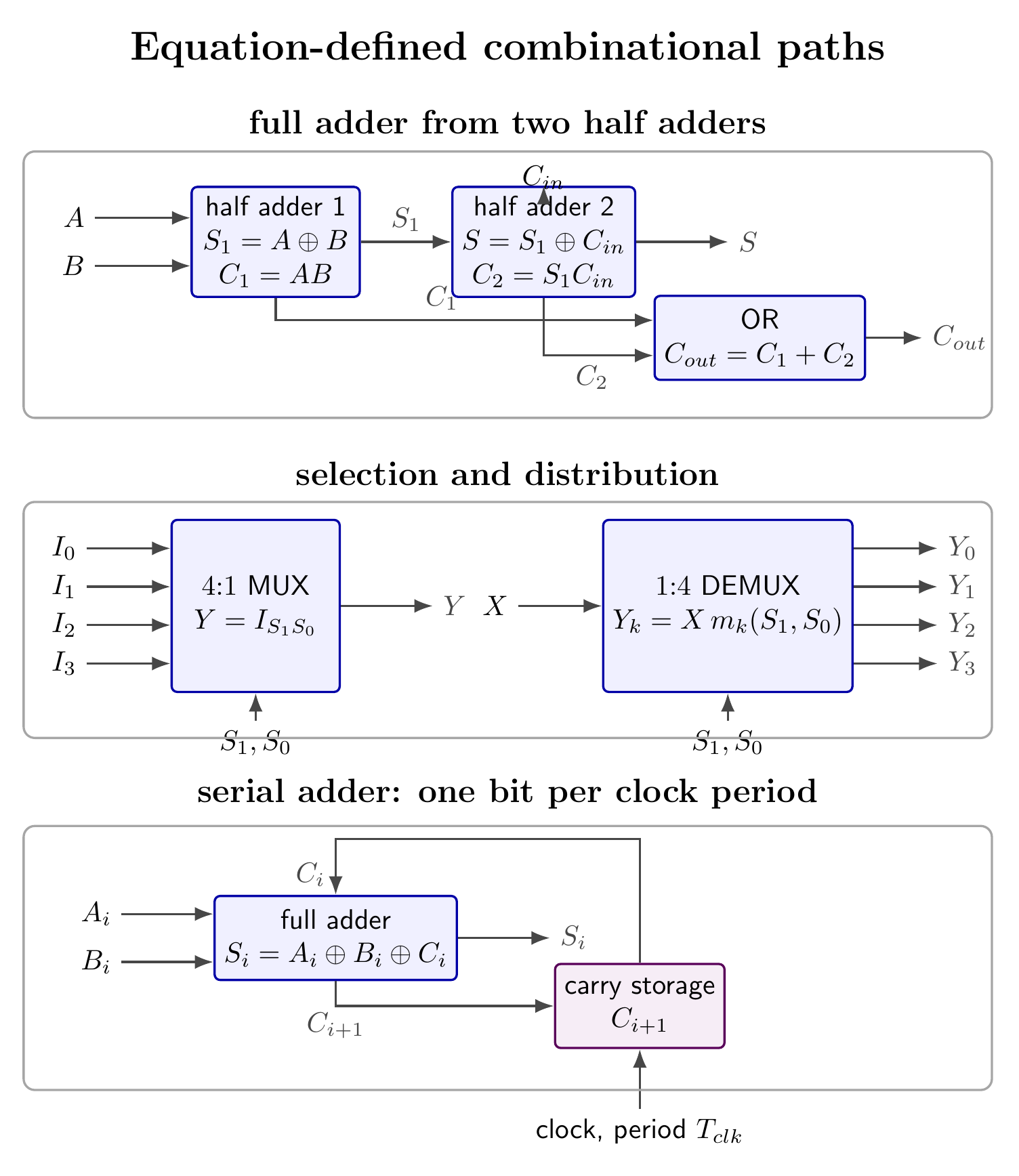
If the storage element has clock-to-output delay $t_{cq}$, the full adder has worst-case delay $t_{comb}$, and the storage input needs setup time $t_{su}$, a safe clock period satisfies
\[T_{clk}\ge t_{cq}+t_{comb}+t_{su}.\]All four quantities have units of time; their reciprocal clock frequency is $f_{clk}=1/T_{clk}$ in hertz.
Half subtractor and full subtractor
A half subtractor represents
\[A-B=D-2B_{out}.\]The difference bit is 1 when $A\ne B$, and a borrow is needed only for $0-1$:
\[D=A\oplus B,\qquad B_{out}=\overline AB.\]For a full subtractor, a first half subtractor gives
\[D_1=A\oplus B,\qquad B_1=\overline AB,\]and subtracting $B_{in}$ from $D_1$ gives
\[D=D_1\oplus B_{in},\qquad B_2=\overline{D_1}B_{in}.\]Therefore
\[\boxed{D=A\oplus B\oplus B_{in}},\] \[\boxed{B_{out}=\overline AB+B_{in}\,\overline{(A\oplus B)}}.\]The arithmetic identity for every input row is
\[A-B-B_{in}=D-2B_{out}.\]Digital comparator
For one bit, the mutually exclusive outputs are
\[G=A\overline B,\qquad E=AB+\overline A\,\overline B,\qquad L=\overline AB,\]for $A>B$, $A=B$, and $A<B$. They obey $G+E+L=1$.
For $n$-bit words, comparison begins at the most significant bit. Define $g_i=A_i\overline B_i$, $l_i=\overline A_iB_i$, and $e_i=A_iB_i+\overline A_i\overline B_i$. Then
\[E=\prod_{i=0}^{n-1}e_i,\] \[G=g_{n-1}+e_{n-1}g_{n-2}+\cdots+e_{n-1}e_{n-2}\cdots e_1g_0,\]and $L$ is obtained by replacing every $g_i$ with $l_i$. A lower bit matters only if all more significant bits are equal.
TTL and CMOS logic families
TTL and CMOS gates can implement the same Boolean truth table but use different device structures and electrical limits.
| Property | TTL | CMOS |
|---|---|---|
| switching devices | bipolar transistors | complementary MOS transistors |
| input current | finite base-current loading | very small steady gate current |
| steady power | appreciable bias current | ideally small except leakage |
| dynamic power | switching contribution | approximately $P_{dyn}=\alpha C_LV_{DD}^{2}f$ |
| input impedance | lower | higher |
| valid levels | family data specify $V_{IL},V_{IH},V_{OL},V_{OH}$ | thresholds scale with family and $V_{DD}$ |
Voltage quantities are measured in volts. The guaranteed noise margins are
\[NM_H=V_{OH(min)}-V_{IH(min)},\] \[NM_L=V_{IL(max)}-V_{OL(max)}.\]Both must be positive for one gate’s guaranteed output to be recognized by the next. Propagation delays $t_{PLH}$ and $t_{PHL}$ describe low-to-high and high-to-low output transitions, commonly summarized by
\[t_{pd}=\frac{t_{PLH}+t_{PHL}}2.\]The load capacitance $C_L$ is in farads, $V_{DD}$ in volts, $f$ in hertz, and the CMOS switching expression therefore has units of watts. TTL and CMOS labels alone do not guarantee compatible thresholds; compatibility is decided by the specified input and output ranges.
Solved Problems
1. Realize a function with a 4-to-1 multiplexer
Use $A,B$ as the select inputs of a 4-to-1 multiplexer to realize
\[F(A,B,C)=\Sigma m(1,2,6,7).\]For each fixed value of $AB$, inspect the two rows obtained as $C$ changes:
| $AB$ | $F(C=0)$ | $F(C=1)$ | required data input |
|---|---|---|---|
| 00 | 0 | 1 | $I_0=C$ |
| 01 | 1 | 0 | $I_1=\overline C$ |
| 10 | 0 | 0 | $I_2=0$ |
| 11 | 1 | 1 | $I_3=1$ |
Thus connect
\[\boxed{I_0=C,\quad I_1=\overline C,\quad I_2=0,\quad I_3=1}.\]Substitution in the multiplexer equation produces 1 only for input rows $1,2,6,7$. All variables are logic levels and therefore dimensionless.
2. Trace a four-bit ripple addition
Add \(A=1011_2\) and \(B=0110_2\) with \(C_0=0\). At each position use \(A_i+B_i+C_i=S_i+2C_{i+1}\), beginning with the least significant bit:
| $i$ | $A_i$ | $B_i$ | $C_i$ | $S_i$ | $C_{i+1}$ |
|---|---|---|---|---|---|
| 0 | 1 | 0 | 0 | 1 | 0 |
| 1 | 1 | 1 | 0 | 0 | 1 |
| 2 | 0 | 1 | 1 | 0 | 1 |
| 3 | 1 | 0 | 1 | 0 | 1 |
Consequently
\[\boxed{C_4S_3S_2S_1S_0=10001_2=17_{10}}.\]The decimal check is $11+6=17$. No signed interpretation was specified, so this is an unsigned, dimensionless addition; retaining $C_4$ prevents loss of the fifth output bit.
Descriptive Questions
- How can the functional completeness of NAND and NOR each be proved by constructing NOT, AND, and OR from only one gate type?
- How do decoder, encoder, multiplexer, and demultiplexer functions differ in data direction and select conditions?
- How are the full-adder and full-subtractor equations derived from their one-bit arithmetic identities?
- How do propagation delay, setup time, noise margin, and capacitive switching power constrain a digital system?
Numerical Problems
-
A 3-to-8 active-high decoder receives $A_2A_1A_0$. Specify the output connections needed to realize $F=\Sigma m(1,4,6)$.
Answer: $F=D_1+D_4+D_6$.
-
Evaluate a full subtractor for $A=0$, $B=1$, and $B_{in}=1$, and verify its arithmetic identity.
Answer: $D=0$, $B_{out}=1$, and $0-1-1=0-2(1)=-2$.
-
A serial adder has $t_{cq}=2.2\ \mathrm{ns}$, $t_{comb}=6.5\ \mathrm{ns}$, and $t_{su}=1.3\ \mathrm{ns}$. Find the minimum safe period and maximum clock frequency.
Answer: $T_{clk,min}=10.0\ \mathrm{ns}$; $f_{clk,max}=100\ \mathrm{MHz}$.
-
A receiving gate specifies $V_{IH(min)}=3.5\ \mathrm V$ and $V_{IL(max)}=1.5\ \mathrm V$; its driver guarantees $V_{OH(min)}=4.4\ \mathrm V$ and $V_{OL(max)}=0.4\ \mathrm V$. Find both noise margins.
Answer: $NM_H=0.9\ \mathrm V$ and $NM_L=1.1\ \mathrm V$.
-
Estimate CMOS dynamic power for $\alpha=0.20$, $C_L=30\ \mathrm{pF}$, $V_{DD}=3.3\ \mathrm V$, and $f=50\ \mathrm{MHz}$.
Answer: $P_{dyn}=3.267\ \mathrm{mW}$.
-
A six-bit comparator receives $A=101101_2$ and $B=101011_2$. State its three outputs $(G,E,L)$.
Answer: $(G,E,L)=(1,0,0)$ because \(45_{10}>43_{10}\).
Editable TikZ source · Maxima verification worksheet
References
- Combinational logic.
- M. Morris Mano and Michael D. Ciletti, Digital Design: With an Introduction to the Verilog HDL, VHDL, and SystemVerilog, 6th ed., Chapters 3–5, Pearson.
- Thomas L. Floyd, Digital Fundamentals, 11th ed., Chapters 5–9, Pearson.


Discussion