

27 Jul 2025
Registers, Memory Devices, and Microprocessors
SR and JK storage, clocking, synchronizers, timers, counters, shift registers, ROM/RAM organization, and 4- to 32-bit architectures including 8085 and 8086.
A sequential circuit stores a state. If $Q_n$ is the state before the active clock event and $Q_{n+1}$ the state after it, a flip-flop is described by a next-state function of its inputs and $Q_n$. This notation separates logic from timing: the logical update occurs at the active event, while the electrical output appears after the clock-to-output delay $t_{cq}$.
SR storage and clocking
An active-high cross-coupled NOR SR latch has set input $S$, reset input $R$, and complementary outputs $Q,\overline Q$. Its allowed-state table is
| $S$ | $R$ | $Q_{n+1}$ | operation |
|---|---|---|---|
| 0 | 0 | $Q_n$ | hold |
| 0 | 1 | 0 | reset |
| 1 | 0 | 1 | set |
| 1 | 1 | invalid | both NOR outputs are forced low |
For the allowed rows,
\[\boxed{Q_{n+1}=S+\overline R\,Q_n},\qquad SR\ne1.\]For example, when $S=R=0$ this gives $Q_{n+1}=Q_n$; when $R=1$ it gives zero; and when $S=1,R=0$ it gives one.
A clocked SR latch gates its inputs:
\[S_g=CS,\qquad R_g=CR.\]When $C=0$, $S_g=R_g=0$ and the state holds. When $C=1$, the latch responds to $S,R$ throughout the high level. It is therefore level-sensitive, not edge-triggered.
JK, master-slave, and edge-triggered flip-flops
The JK flip-flop replaces the forbidden SR command with feedback-controlled toggling:
| $J$ | $K$ | $Q_{n+1}$ | operation |
|---|---|---|---|
| 0 | 0 | $Q_n$ | hold |
| 0 | 1 | 0 | reset |
| 1 | 0 | 1 | set |
| 1 | 1 | $\overline Q_n$ | toggle |
All four rows are represented by the characteristic equation
\[\boxed{Q_{n+1}=J\overline Q_n+\overline KQ_n}.\]For $J=K=1$, it becomes $Q_{n+1}=\overline Q_n$. A level-sensitive JK circuit could then change repeatedly during a clock level if the feedback completed more than once. A master-slave connection prevents that race: the master accepts inputs during one clock level, while the slave accepts the master’s state during the complementary level. The two latches are never transparent simultaneously.
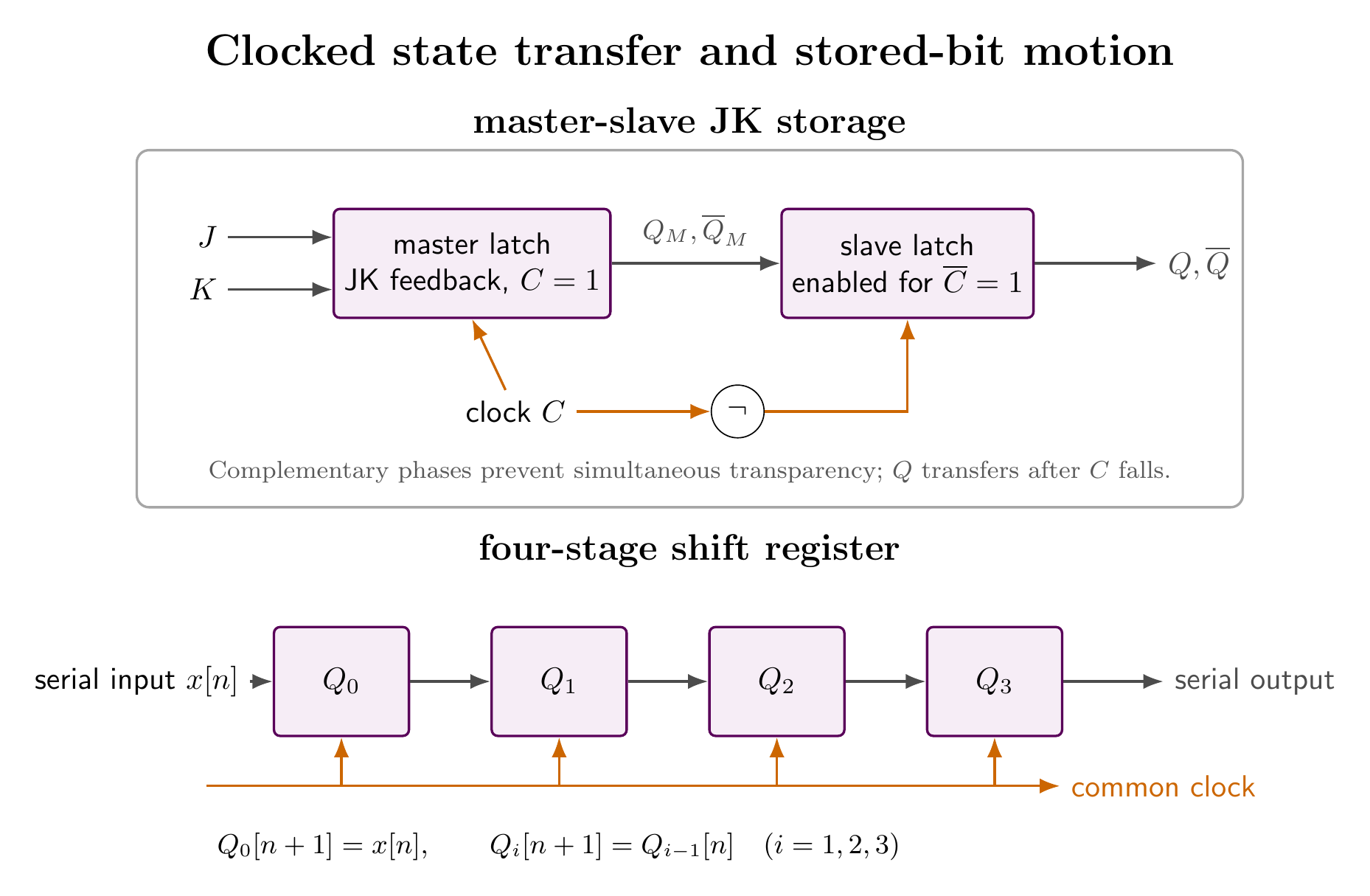
With a master active for $C=1$ and a slave active for $C=0$, the external output changes after the falling edge. Reversing the phases produces a rising-edge device. An edge-triggered flip-flop is denoted by a clock triangle; a clock bubble together with the triangle denotes a falling-edge trigger.
The data inputs must remain stable for setup time $t_{su}$ before the active edge and hold time $t_h$ after it. The new output becomes valid after $t_{cq}$. These are time intervals, normally specified in nanoseconds. Violating setup or hold time can leave the internal state temporarily metastable rather than immediately at a guaranteed 0 or 1.
Synchronizer
An input unrelated to the receiving clock can change inside the setup/hold aperture. A synchronizer passes that input through two cascaded edge-triggered storage stages clocked by the receiving clock. The first stage may become metastable; the second samples it one period later, allowing a resolution time approximately
\[t_{res}\simeq T_{clk}-t_{cq}-t_{su}.\]The cascade does not make the metastability probability exactly zero, but greatly reduces the probability that an unresolved level reaches the synchronous logic. The cost is clock-cycle latency.
Timer and counter
A digital timer counts periods of a reference clock. If $N$ periods of frequency $f_{clk}$ are counted, then
\[\boxed{t=NT_{clk}=\frac{N}{f_{clk}}}.\]Here $t$ is in seconds when $f_{clk}$ is in hertz. For $N=2500$ and $f_{clk}=1.0\,\text{MHz}$,
\[t=\frac{2500}{1.0\times10^6}\,\text{s}=2.5\times10^{-3}\,\text{s}=2.5\,\text{ms}.\]An $n$-stage binary counter updates
\[Q_{n+1}=(Q_n+1)\bmod 2^n,\]so it has $2^n$ states from $0$ through $2^n-1$. A modulus-$M$ counter instead cycles through $M$ specified states. In a ripple counter, one stage’s output clocks the next, so transition delays accumulate. In a synchronous counter, all stages share the clock and combinational logic determines which stages toggle; state changes are referenced to the same edge.
Shift register
A shift register moves stored bits by one position at every active edge. For the four-stage arrangement in the figure,
\[Q_0[n+1]=x[n],\qquad Q_i[n+1]=Q_{i-1}[n]\quad(i=1,2,3).\]Because all right-hand sides use the state before the edge, all four updates are simultaneous. Serial input and output use one line each; access to all $Q_i$ provides a parallel word. A register can therefore convert between serial and parallel representation or delay a bit stream by an integer number of clock periods.
ROM, shift-register memory, and RAM
If a memory has $a$ address inputs and stores $w$ bits at each address, it contains
\[2^a\ \text{words},\qquad 2^aw\ \text{bits}.\]For a $4\text{K}\times8$ memory, $4\text{K}=2^{12}$ addresses and
\[2^{12}(8)=32768\ \text{bits}=4096\ \text{bytes}.\]- Read-only memory (ROM): the address decoder selects one stored word for reading. Normal system operation does not alter the contents, so ROM holds fixed tables or program words.
- Shift-register memory: words circulate or move through cascaded storage stages. Access is sequential; if the required word is $k$ positions away, it appears after $kT_{clk}$ rather than after an address decode.
- Random-access memory (RAM): an address can select any word directly for reading or writing. “Random” means that access time does not depend on the word’s position in a serial sequence.
Memory capacity is measured in bits or bytes, address width in bits, access time in seconds, and access rate in transfers per second. These quantities describe different properties and must not be interchanged.
Microprocessor architecture and word size
A microprocessor repeatedly performs a fetch-decode-execute sequence:
- The program counter places the next instruction address on the address path.
- Memory returns an opcode on the data path.
- The instruction register and decoder generate control signals.
- Registers supply operands to the arithmetic-logic unit.
- The result returns to a register or memory, flags record selected result properties, and the program counter advances or branches.
The necessary components are therefore an ALU, register set, program counter, instruction decoder, timing/control logic, address and data interfaces, and connections to memory and input/output. A stack pointer, condition flags, interrupt control, and clock circuitry support program sequencing and external events.
The processor word size is the natural width of its ALU and principal data registers. For an $n$-bit word,
\[0\le N_{unsigned}\le2^n-1,\] \[-2^{n-1}\le N_{signed}\le2^{n-1}-1.\]| word size | unsigned range | two’s-complement signed range |
|---|---|---|
| 4 bit | $0$ to $15$ | $-8$ to $7$ |
| 8 bit | $0$ to $255$ | $-128$ to $127$ |
| 16 bit | $0$ to $65535$ | $-32768$ to $32767$ |
| 32 bit | $0$ to $4294967295$ | $-2147483648$ to $2147483647$ |
A 4-bit processor handles one hexadecimal digit naturally; 8-, 16-, and 32-bit processors handle progressively wider data words per ALU operation. Word size does not by itself determine address space. If the address path has $a$ bits and each address selects one byte, the byte-address space is $2^a$ bytes.
Brief 8085 architecture
The 8085 is an 8-bit microprocessor with an 8-bit ALU and data interface. Its 16-bit address interface selects
\[2^{16}=65536\ \text{byte locations}=64\ \text{KiB}.\]Its principal components are the accumulator $A$, temporary ALU storage, flags $S,Z,AC,P,CY$, six 8-bit registers $B,C,D,E,H,L$ that can form the pairs $BC,DE,HL$, and the 16-bit program counter and stack pointer. The instruction register/decoder and timing-control section coordinate transfers; interrupt and serial-control sections handle external requests and one-bit serial signals.
The high address bits use $A_{15}$-$A_8$. The pins $AD_7$-$AD_0$ carry the low address during the first part of a machine cycle and data afterward, so an external latch preserves the low address. This multiplexing changes pin use with time; it does not reduce the 16-bit address range.
Brief 8086 architecture
The 8086 is a 16-bit microprocessor with a 16-bit ALU and external data path. A 20-bit address path selects
\[2^{20}=1048576\ \text{bytes}=1\ \text{MiB}.\]Its architecture separates an execution unit from a bus-interface unit. The execution unit contains the ALU, flags, general registers $AX,BX,CX,DX$, pointer/index registers $SP,BP,SI,DI$, and instruction decoding. The bus-interface unit contains segment registers $CS,DS,SS,ES$, instruction pointer $IP$, address generation, bus control, and a six-byte instruction prefetch queue.
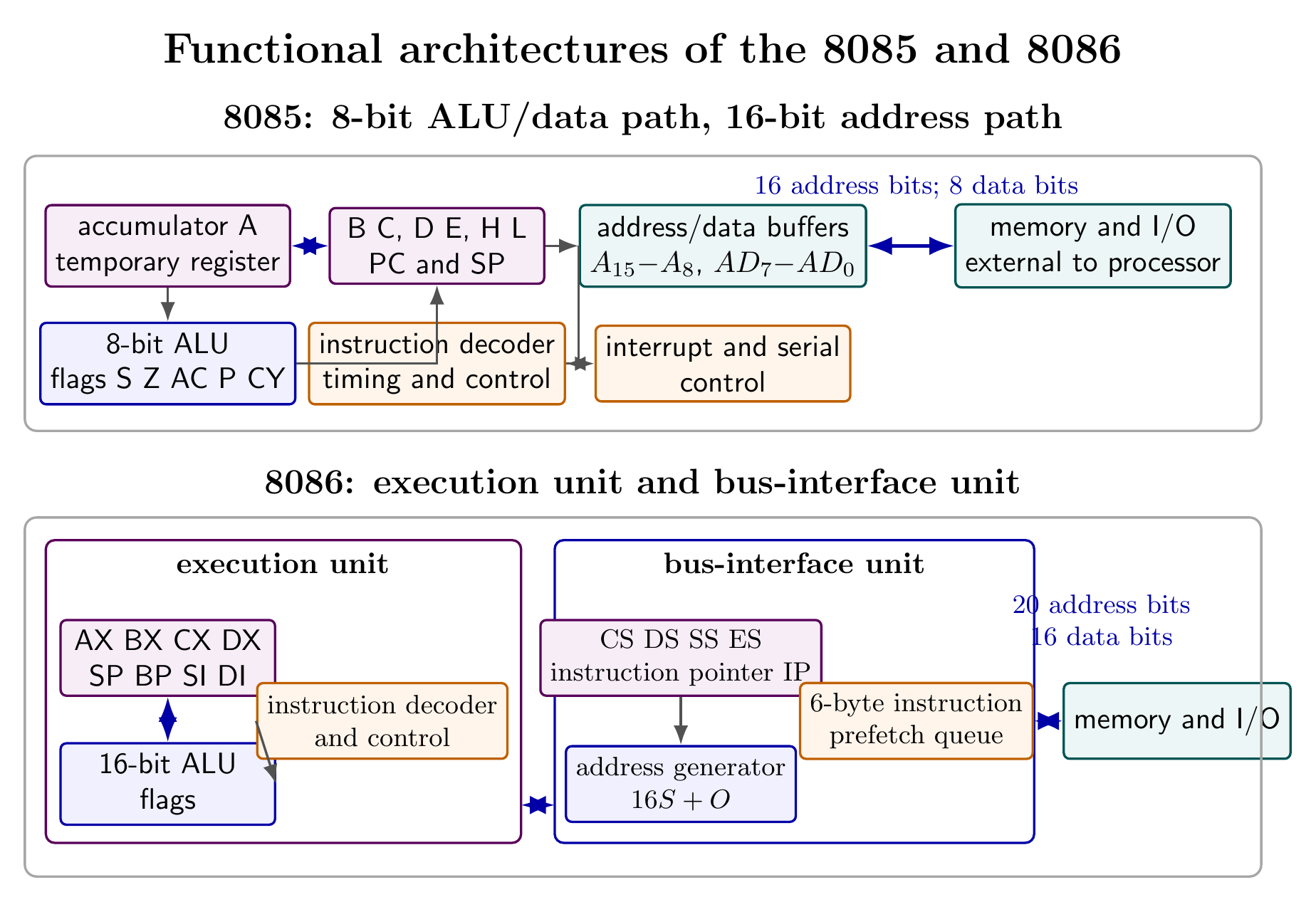
For segment value $S$ and 16-bit offset $O$, the physical address is
\[\boxed{A_{phys}=16S+O\pmod{2^{20}}}.\]For example,
\[1234_{16}\times10_{16}+5678_{16}=179B8_{16}.\]Multiplication by $10_{16}$ shifts the segment left four bits, so segment starts are separated by 16 bytes and different segment:offset pairs can identify the same physical byte. The prefetch queue permits the bus interface to fetch instruction bytes while the execution unit works, but a control transfer must begin fetching from the new instruction address.
Solved Problems
1. Trace a JK flip-flop command sequence
An edge-triggered JK flip-flop starts at $Q_0=0$. Successive clock edges apply
\[(J,K)=(1,0),(0,0),(1,1),(0,1),(1,1).\]Apply $Q_{n+1}=J\overline Q_n+\overline KQ_n$ after each edge:
| edge | $(J,K)$ | operation | state after edge |
|---|---|---|---|
| 1 | $(1,0)$ | set | 1 |
| 2 | $(0,0)$ | hold | 1 |
| 3 | $(1,1)$ | toggle | 0 |
| 4 | $(0,1)$ | reset | 0 |
| 5 | $(1,1)$ | toggle | 1 |
Thus the state sequence is
\[\boxed{Q_1,Q_2,Q_3,Q_4,Q_5=1,1,0,0,1}.\]The sequence is dimensionless and assumes each input pair satisfies setup and hold time at its edge; propagation delay changes when the new level becomes observable, not the logical sequence.
2. Form and interpret an 8086 physical address
Find the physical address represented by 2A3C:4F20 and give one alias with zero offset. The segment contribution is shifted left by four bits:
Adding the offset,
\[\begin{aligned} A_{phys} &=2A3C0_{16}+4F20_{16}\\ &=\boxed{2F2E0_{16}}. \end{aligned}\]This is below $FFFFF_{16}$, so reduction modulo $2^{20}$ changes nothing. Since \(2F2E_{16}\times10_{16}=2F2E0_{16}\), 2F2E:0000 is an alias. Physical addresses count bytes; the segment and offset are dimensionless hexadecimal integers.
Descriptive Questions
- How is the JK characteristic equation derived, and how does master-slave clocking remove race-around?
- How do ripple and synchronous counters differ in state timing, accumulated delay, and maximum clock rate?
- How are ROM, RAM, and shift-register memory distinguished by addressing method, access order, and write capability?
- How do the 8085 and 8086 differ in data path, address formation, register organization, and instruction-fetch mechanism?
Numerical Problems
-
A two-stage synchronizer runs with $T_{clk}=20\ \mathrm{ns}$, $t_{cq}=2.0\ \mathrm{ns}$, and second-stage setup time $t_{su}=1.5\ \mathrm{ns}$. Estimate its available metastability-resolution time.
Answer: $t_{res}\simeq16.5\ \mathrm{ns}$.
-
Find the overflow interval of a 16-bit binary timer clocked at $2.00\ \mathrm{MHz}$, starting from zero.
Answer: $2^{16}/(2.00\times10^6)=32.768\ \mathrm{ms}$.
-
What is the minimum number of flip-flops for a modulus-10 counter, and how many binary states remain unused?
Answer: $4$ flip-flops; $16-10=6$ unused states.
-
Let the shift-register state be ordered as $(Q_0,Q_1,Q_2,Q_3)$, initially $(0,1,0,1)$. Under $Q_0[n+1]=x[n]$ and $Q_i[n+1]=Q_{i-1}[n]$, apply serial inputs $1,0,1$.
Answer: final state $(1,0,1,0)$.
-
Determine the address-input count and total capacity of a $32\mathrm K\times8$ RAM.
Answer: $15$ address inputs; $262144$ bits $=32768$ bytes $=32\ \mathrm{KiB}$.
-
An 8085 system maps an $8\ \mathrm{KiB}$ byte-addressed memory from
8000H. Find the inclusive final address.Answer:
9FFFH.
Editable sequential-storage TikZ · Editable architecture TikZ · Maxima verification worksheet
References
- Microprocessor.
- Ramesh S. Gaonkar, Microprocessor Architecture, Programming, and Applications with the 8085, 6th ed., Chapters 1–3, Penram International.
- Barry B. Brey, The Intel Microprocessors: Architecture, Programming, and Interfacing, 8th ed., Chapters 1–3, Pearson.


Discussion