05 Mar 2026
Basic Electronics: Intrinsic and Extrinsic Semiconductors
Intrinsic and extrinsic semiconductors, band model, doping, n-type and p-type materials, and exam-style answer points.
A semiconductor is a material whose electrical conductivity lies between that of a conductor and an insulator. Silicon and germanium are the standard examples. Their conductivity is small at low temperature, but it increases when thermal energy, light, or impurities create mobile charge carriers.
In the open elective syllabus, this topic begins with the distinction between intrinsic and extrinsic semiconductors. This distinction is essential before studying p-n junctions, diodes, LEDs, transistors, and FETs.
Bond picture
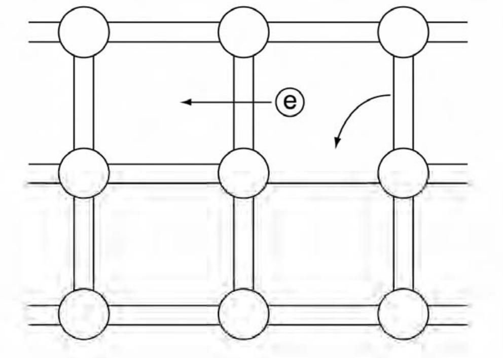
Silicon has four valence electrons. In a pure silicon crystal, each atom shares these electrons with neighboring atoms and forms covalent bonds. At very low temperature, nearly all bonds are complete, so there are very few free carriers.
When temperature increases, some covalent bonds break. This produces:
- a free electron in the crystal,
- a vacancy in a bond, called a hole.
A hole behaves like a positive charge carrier because a neighboring electron can move into the vacancy, making the hole appear to move in the opposite direction.
Band picture
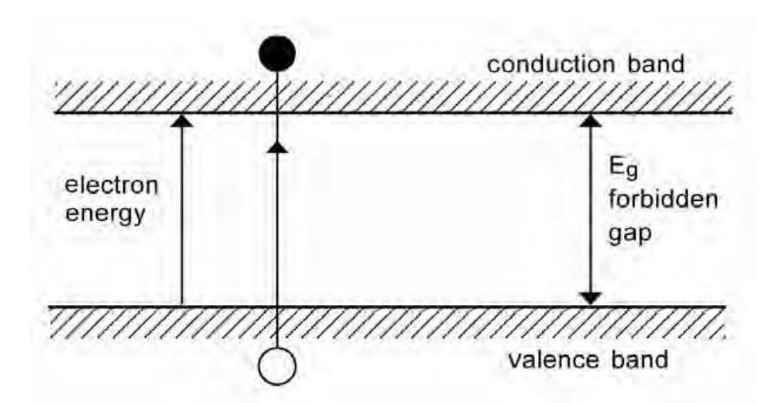
The band model explains semiconductors using energy bands. The valence band contains electrons bound in covalent bonds. The conduction band contains electrons free to move through the crystal.
The energy gap between the valence band and conduction band is called the forbidden gap or band gap. In a semiconductor this gap is small enough that electrons can be thermally excited from the valence band to the conduction band.
Intrinsic semiconductor
An intrinsic semiconductor is a pure semiconductor without intentional impurity doping. In an intrinsic semiconductor:
- the number of free electrons is equal to the number of holes;
- conduction is due to both electrons and holes;
- conductivity increases with temperature;
- silicon and germanium in pure form are standard examples.
If $n$ is the electron concentration and $p$ is the hole concentration, then for an intrinsic semiconductor,
\[n=p=n_i,\]where $n_i$ is the intrinsic carrier concentration.
Extrinsic semiconductor
An extrinsic semiconductor is formed by adding a small amount of suitable impurity to a pure semiconductor. This process is called doping. Doping greatly changes the number of mobile charge carriers and hence increases conductivity.
There are two types of extrinsic semiconductors:
| Type | Dopant | Majority carriers | Minority carriers |
|---|---|---|---|
| n-type | Pentavalent impurity such as P, As, Sb | Electrons | Holes |
| p-type | Trivalent impurity such as B, Al, Ga | Holes | Electrons |
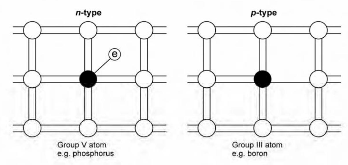
n-type semiconductor
When a pentavalent impurity atom is added to silicon, four of its five valence electrons form covalent bonds with neighboring silicon atoms. The fifth electron is weakly bound and becomes available for conduction.
Thus in an n-type semiconductor:
- electrons are majority carriers;
- holes are minority carriers;
- the impurity atom is called a donor;
- the material remains electrically neutral as a whole.
p-type semiconductor
When a trivalent impurity atom is added to silicon, it forms only three covalent bonds. One bond remains incomplete, creating a hole.
Thus in a p-type semiconductor:
- holes are majority carriers;
- electrons are minority carriers;
- the impurity atom is called an acceptor;
- the material remains electrically neutral as a whole.
Comparison
| Point | Intrinsic semiconductor | Extrinsic semiconductor |
|---|---|---|
| Purity | Pure material | Doped material |
| Carrier concentration | Electrons and holes equal | One carrier type dominates |
| Conductivity | Low | Higher |
| Control | Mainly temperature dependent | Controlled by impurity doping |
| Examples | Pure Si, pure Ge | n-type Si, p-type Si |
University questions
The 2019 open elective paper asked: “What is intrinsic semiconductor?” A complete short answer should include purity, equal electron-hole concentration, temperature dependence, and one example.
Practice questions from this syllabus:
- Define intrinsic semiconductor.
- Distinguish intrinsic and extrinsic semiconductors.
- Explain n-type and p-type semiconductors.
- What are majority and minority carriers?
- Explain donor and acceptor impurities.
Answer points
- Start with the definition of semiconductor.
- State that intrinsic means pure and extrinsic means doped.
- Mention electrons and holes as charge carriers.
- For n-type, write donor impurity and electrons as majority carriers.
- For p-type, write acceptor impurity and holes as majority carriers.
Discussion