06 Mar 2026
Basic Electronics: p-n Junction Diode
Formation of a p-n junction, depletion region, forward and reverse bias, diode characteristics, and exam-style notes.
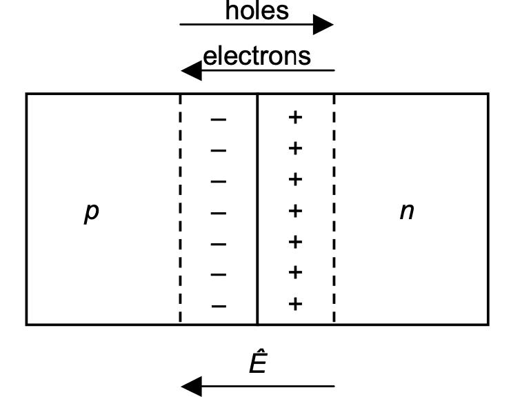
A p-n junction is formed when a p-type semiconductor and an n-type semiconductor are joined in a single crystal. The p-side contains holes as majority carriers, while the n-side contains electrons as majority carriers.
The junction is important because it allows current to pass easily in one direction but opposes current in the opposite direction. This one-way behavior is the basic principle of a semiconductor diode.
Formation of depletion region
Immediately after the p-type and n-type regions are joined, electrons from the n-side diffuse into the p-side and recombine with holes. Similarly, holes from the p-side diffuse into the n-side and recombine with electrons.
This recombination leaves behind fixed ionized donor and acceptor atoms near the junction. Since this region has very few mobile carriers, it is called the depletion region.
Potential barrier
The fixed ions in the depletion region create an electric field. This electric field opposes further diffusion of electrons and holes. The corresponding potential difference across the junction is called the barrier potential.
At equilibrium:
- diffusion tendency pushes majority carriers across the junction;
- the electric field opposes further diffusion;
- no net current flows through the junction.
Forward bias
In forward bias, the p-side is connected to the positive terminal and the n-side to the negative terminal of a battery.
Forward bias reduces the barrier potential and narrows the depletion region. Majority carriers can cross the junction easily, so the diode conducts current.
Reverse bias
In reverse bias, the p-side is connected to the negative terminal and the n-side to the positive terminal.
Reverse bias increases the barrier potential and widens the depletion region. Majority carriers cannot cross the junction easily, so only a very small reverse saturation current flows due to minority carriers.
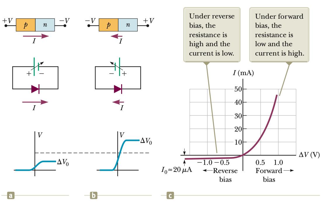
V-I characteristic
The V-I characteristic of a p-n junction diode has two main regions:
| Bias | Depletion region | Current behavior |
|---|---|---|
| Forward bias | Narrows | Current rises rapidly after cut-in voltage |
| Reverse bias | Widens | Very small reverse saturation current |
The diode therefore behaves like a rectifying device. It is used to convert alternating current into unidirectional current in rectifier circuits.
Characteristics of a p-n junction
In a short-note answer on p-n junction characteristics, include:
- formation of depletion layer;
- barrier potential;
- forward bias behavior;
- reverse bias behavior;
- one-way conduction;
- rectifier application.
University questions
The 2019 open elective paper asked for a short note on “Characteristics of PN junction.” A good answer should draw the V-I characteristic and explain forward and reverse bias qualitatively.
Practice questions:
- Explain the formation of a p-n junction.
- What is the depletion region?
- Distinguish forward bias and reverse bias.
- Draw and explain the V-I characteristic of a p-n junction diode.
- Why is a p-n junction diode used as a rectifier?
Answer points
- Begin with p-type and n-type regions.
- Explain diffusion and recombination.
- Mention fixed ions and depletion layer.
- Explain the effect of forward and reverse bias.
- End with the rectifying action of the diode.
Discussion