

13 May 2025
8085 Bus Timing Diagrams
Address-data demultiplexing and exact opcode-fetch, memory, I/O and wait-state timing on the 8085 system bus.
An 8085 timing diagram states not only what transfer occurs, but also when the address, data and control signals are valid. The processor has a dedicated high-order address bus $A_{15}$-$A_8$ and a multiplexed low-order address/data bus $AD_7$-$AD_0$. A correct interface must preserve the low address after the shared pins change function, decode whether the transfer is memory or I/O, and enable the selected device only inside the valid data interval.
Signal names with an overbar are active low. Thus $\overline{\mathrm{RD}}=0$ commands a selected device to drive the data bus, and $\overline{\mathrm{WR}}=0$ commands it to accept CPU data. ALE is active high. IO/M is low for a memory transaction and high for an I/O transaction.
Demultiplexing the lower address
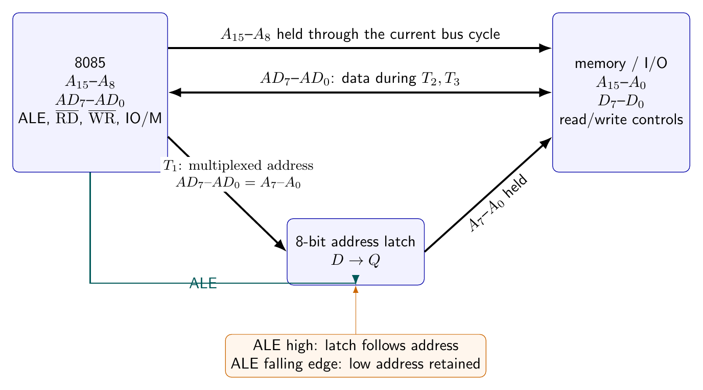
During $T_1$ of every bus machine cycle, $A_{15}$-$A_8$ carries the high address and $AD_7$-$AD_0$ carries $A_7$-$A_0$. ALE rises during this address phase. An external transparent latch, such as the latch integrated into Intel’s 8155/8355/8755 family or a separate eight-bit latch, follows the AD inputs while enabled. The falling edge of ALE closes the latch, so its outputs retain $A_7$-$A_0$ throughout the remainder of the cycle.
After the address phase, the CPU releases or drives $AD_7$-$AD_0$ according to the transfer direction. For a read, the selected memory or peripheral drives these lines. For a write, the CPU drives them. The latched low address is therefore essential: connecting a memory address input directly to AD would replace its address with the data byte during $T_2$ and $T_3$.
Status and cycle identification
The status outputs $S_1,S_0$ encode the basic bus action: 11 fetch, 10 read, 01 write and 00 halt. Combining them with IO/M distinguishes the common cycles.
IO/M |
$S_1S_0$ | Cycle |
|---|---|---|
| 0 | 11 | opcode fetch from memory |
| 0 | 10 | memory read |
| 0 | 01 | memory write |
| 1 | 10 | I/O read |
| 1 | 01 | I/O write |
Status is useful for decoding and instrumentation, but the active-low control outputs establish the actual transfer interval. IO/M=0 and $\overline{\mathrm{RD}}=0$ identifies a memory read; IO/M=1 and $\overline{\mathrm{WR}}=0$ identifies an I/O write. $\overline{\mathrm{INTA}}$ replaces the normal read control during the instruction cycle following an accepted INTR request.
Opcode-fetch timing
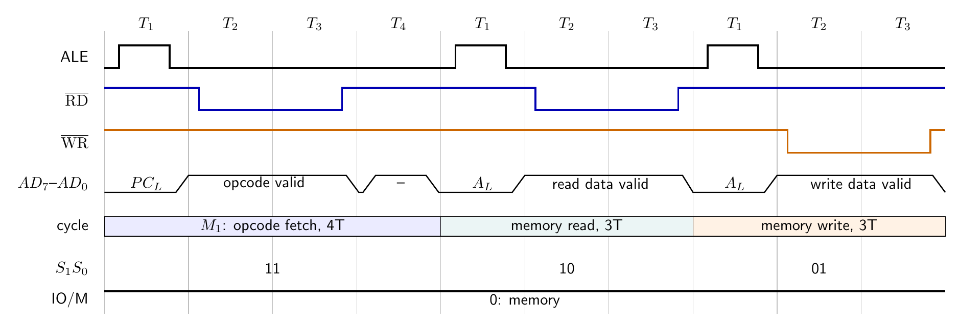
The first machine cycle of an instruction is $M_1$, the opcode fetch. Its standard length is four T-states.
- In $T_1$, the PC address appears on the address buses and ALE pulses high.
IO/Mindicates memory and $S_1S_0=11$ identifies fetch. - In $T_2$, the low bus changes from address to input data and $\overline{\mathrm{RD}}$ goes low. The addressed memory must begin driving the opcode.
- In $T_3$, the opcode is valid and is accepted by the CPU. $\overline{\mathrm{RD}}$ returns high, ending the device’s bus drive.
- In $T_4$, the processor decodes the opcode and performs the internal action needed to schedule the rest of the instruction.
The fourth state distinguishes a normal opcode fetch from an ordinary three-state data read. MOV B,C, ADD D and NOP finish after this one four-state cycle. When decode finds an immediate byte or memory operand, $M_2$ begins with another address phase.
Memory-read timing
A basic memory-read cycle occupies $T_1,T_2,T_3$. The 16-bit address is presented in $T_1$, ALE latches its low byte, and IO/M=0, $S_1S_0=10$. During $T_2$ the CPU makes the multiplexed bus available for input and asserts $\overline{\mathrm{RD}}$. Memory drives the selected byte after its access delay. The byte must be valid for the processor’s specified setup interval before the sampling edge in $T_3$ and held for the required interval afterward. Once $\overline{\mathrm{RD}}$ returns high, the memory must release the bus.
An operand read and an instruction-byte read use this same bus form. Their logical roles differ: MVI A,32H uses its $M_2$ read to obtain immediate data from PC, while MOV A,M uses $M_2$ to obtain an operand from the address held in HL. Each instruction has $4+3=7$ basic T-states.
Memory-write timing
A memory write also begins with the address and ALE in $T_1$, but IO/M=0, $S_1S_0=01$. In $T_2$ the CPU drives the output data on $AD_7$-$AD_0$ and asserts $\overline{\mathrm{WR}}$ low. Address and data remain stable through the active control interval. Intel specifies that the selected location accepts the data at the trailing, low-to-high edge of $\overline{\mathrm{WR}}$; the CPU retains data briefly after that edge to meet hold time.
For MOV M,A, the opcode fetch is followed by one memory-write cycle, giving 2 machine cycles and 7 T-states. MVI M,32H first reads its immediate byte and then writes it at HL, giving OF + MR + MW = $4+3+3=10$ T-states.
I/O read and write cycles
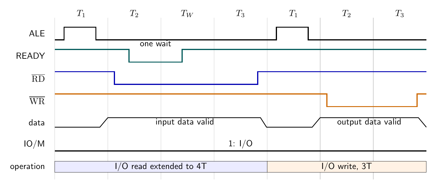
The electrical direction and active control shapes of I/O cycles parallel their memory counterparts, but IO/M=1. IN 42H has opcode DBH followed by port byte 42H. It uses an opcode fetch, a memory read to obtain the second instruction byte, and an I/O read: 2 bytes, 3 machine cycles and 10 T-states. During the I/O cycle the port number is duplicated on both halves of the address bus, so 42H appears as 4242H. The addressed port drives $AD_7$-$AD_0$ while $\overline{\mathrm{RD}}$ is active, and the CPU transfers the byte to the accumulator.
OUT 42H has opcode D3H and the same 2-byte, 3-cycle, 10-state structure. In its final I/O-write cycle the duplicated port address is present, the accumulator byte is driven on AD, and $\overline{\mathrm{WR}}$ is active. Memory and peripherals must not both respond: IO/M belongs in the chip-select or control decoding.
The port address is eight bits even though the physical address presentation is sixteen bits. Consequently the standard isolated-I/O space contains 256 port numbers, 00H through FFH. This differs from memory-mapped I/O, where ordinary memory instructions and the full 16-bit memory address are used and IO/M remains low.
READY and the wait state
READY permits a slower device to extend a transfer. If it is low at the required sampling instant in a read or write cycle, the 8085 inserts a wait state $T_W$ between $T_2$ and $T_3$. It tests readiness again and can insert further waits until READY is high. During the extension the address remains valid and the active read or write control remains asserted; the transfer is not restarted.
One wait state adds exactly one clock period. Thus MOV A,M is normally 7 T-states. If its operand read contains two waits, it takes 9 T-states. At $3\,\text{MHz}$ this is $3.000\,\mu\text{s}$ instead of $2.333\,\mu\text{s}$. The opcode still occupies one byte and the instruction still contains two machine cycles.
Reading a timing diagram rigorously
A waveform should be checked in a fixed order. First identify machine-cycle boundaries and state labels. Then read the address during $T_1$ rather than during the later data phase. Confirm that ALE is a positive pulse and that $\overline{\mathrm{RD}}$ and $\overline{\mathrm{WR}}$ are never simultaneously active in an ordinary transfer. Use IO/M and $S_1S_0$ to classify the cycle. Finally mark the valid data window and determine its owner: the external device owns data during a read; the CPU owns it during a write.
This method also exposes drawing errors. A low-address label continuing across $T_2$ on the raw AD bus is incorrect; only the latch output preserves that address. A write-data window that begins after $\overline{\mathrm{WR}}$ rises cannot meet the trailing-edge requirement. A memory cycle drawn with IO/M=1, or an active-high label RD, reverses the bus meaning.
The timing and signal definitions above follow Intel’s MCS-80 User’s Manual (October 1977), including the 8085 pin definitions and basic system timing, and Intel’s 8080/8085 Assembly Language Programming Manual (November 1978) for instruction cycles and states.
Preparation questions
- Explain why an external latch is required even though the 8085 presents all sixteen address bits during $T_1$.
- Draw the bus ownership of $AD_7$-$AD_0$ during $T_1,T_2,T_3$ for one memory read and one memory write.
- Decompose
IN A5Hinto bytes and machine cycles, and calculate its no-wait T-state count. - Which values of
IO/Mand $S_1S_0$ distinguish opcode fetch, memory write and I/O read? - A
MOV M,Ainstruction encounters three wait states. Find its total time at $2\,\text{MHz}$. - State the instant at which a selected memory device accepts write data and identify the required data-valid intervals around it.
- Diagnose why a circuit that decodes only $A_{15}$-$A_8$ and ignores
IO/Mmay produce bus contention.


Discussion