

05 May 2025
8085 Pinout, Buses, Control and Internal Operation
The 8085 forty-pin interface, multiplexed buses, control and status signals, interrupt pins, and fetch-decode-execute data flow.
The Intel 8085 is an 8-bit microprocessor in a 40-pin package with a 16-bit address interface. It can select
\[2^{16}=65\,536\ \text{memory locations}=64\ \text{KiB},\]from 0000H through FFFFH, and transfer one 8-bit data byte at a time. Providing separate pins for all sixteen address bits and all eight data bits would require twenty-four signals. The 8085 instead uses eight dedicated high-address pins and eight shared lines: AD7–AD0 carry the low address during the first part of a machine cycle and data afterward.
Pin functions and processor operation should be read together. A pin name states an electrical interface; a bus cycle states when it is meaningful; an instruction states why the cycle occurs. The factual baseline used here is Intel’s 8080/8085 Assembly Language Programming Manual and MCS-80 User’s Manual.
Forty-pin organization
The pins form functional groups rather than forty independent signals.
- Address and data:
A15–A8are the high-order address lines.AD7–AD0are multiplexed low-address/data lines. - Bus control and status:
ALE, active-lowRD, active-lowWR,IO/M,S1, andS0identify and control the current transfer. Active-lowINTAacknowledgesINTR. - Clock and reset:
X1,X2,CLK OUT, active-lowRESET IN, andRESET OUTestablish timing and system initialization. - Wait and direct-memory-access handshake:
READY,HOLD, andHLDAcoordinate slow devices and external bus masters. - Interrupts:
TRAP,RST 7.5,RST 6.5,RST 5.5, andINTRrequest service with different priority and masking behavior. - Serial I/O:
SIDis serial input data andSODis serial output data, controlled throughRIMandSIM. - Power:
VCCandVSSprovide the supply and reference.
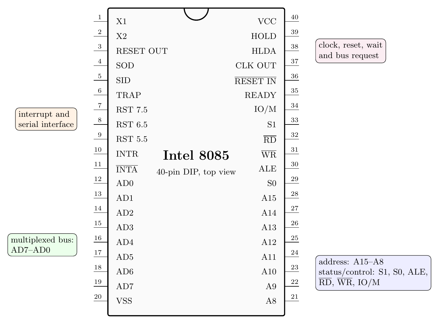
Electrical design must use the exact device-family data sheet for voltage, loading, and timing limits. Logical diagrams alone do not specify permissible fan-out, rise time, or setup and hold margins.
Address, data and control buses
The address bus answers “which location or port?” For a memory transaction, the 16-bit address is
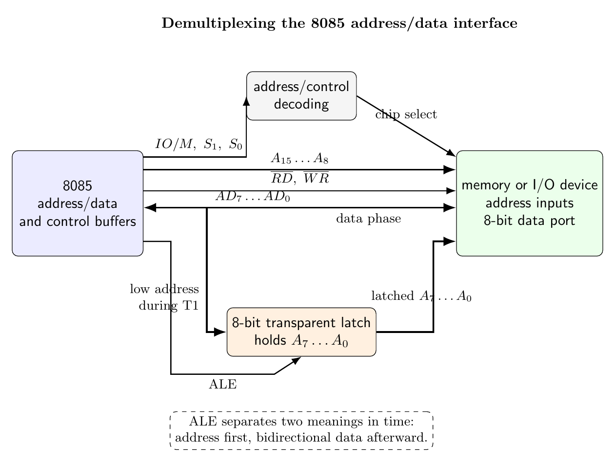
\[A_{15}\ldots A_8\;A_7\ldots A_0.\]The high byte appears on A15–A8. The low byte initially appears on AD7–AD0. Because the same eight pins must later become the bidirectional data bus, an external latch is normally enabled by ALE (address latch enable). While ALE is high the low address is available; when the latch closes, it retains A7–A0 for the remainder of the cycle. The processor can then use AD7–AD0 to read or write data.
The data bus is bidirectional. During a read, the selected memory or peripheral drives a byte toward the processor. During a write, the processor drives a byte outward. Only one enabled device may drive the bus at a time; address decoding and control logic must prevent contention.
The control bus describes the transfer. Active-low RD tells the selected device to drive readable data. Active-low WR tells it to accept processor data. IO/M distinguishes I/O from memory: low identifies a memory cycle and high an I/O cycle. S1 and S0 provide additional machine-cycle status.
| Operation | IO/M |
active control | S1 S0 |
|---|---|---|---|
| opcode fetch | 0 | RD |
11 |
| memory read | 0 | RD |
10 |
| memory write | 0 | WR |
01 |
| I/O read | 1 | RD |
10 |
| I/O write | 1 | WR |
01 |
| interrupt acknowledge | 1 | INTA |
11 |
The opcode fetch is electrically a memory read but has its own status code because the byte is destined for the instruction register. RD and WR must never be asserted together in a normal transfer.
Machine-cycle timing
An instruction is executed as one or more machine cycles, and each machine cycle contains clock periods called T-states. In the first T-state of a bus cycle, the processor presents the address and pulses ALE. For a read cycle it then releases the multiplexed lines for input, asserts active-low RD, and samples the returned data when the timing requirements are satisfied. For a write it drives the output byte and asserts active-low WR so the selected device can store it.
READY allows a device to extend a transfer. If it is not ready when sampled, the processor inserts wait state or states while retaining the relevant address and control conditions. Wait states change execution time but do not change the instruction bytes or architectural result.
The status signals must be interpreted only during their specified valid interval. They describe a machine cycle, not the complete instruction. A three-byte instruction produces several fetch/read cycles; a one-byte MOV A,M still adds a data-memory read because its operand resides at the address in HL.
Clock and reset signals
X1 and X2 connect to the on-chip clock-generator network, commonly with a crystal or an approved external source. The processor derives its internal timing from this oscillator; CLK OUT supplies a related clock to system devices. The oscillator input and processor clock are not automatically the same numerical frequency, so board timing must follow the specified division and device grade.
Driving active-low RESET IN initializes processor control state and clears the program counter so execution begins at address 0000H after reset is released. Interrupt enable is cleared. A robust design holds reset for the required duration after clock and supply become valid. RESET OUT lets the processor’s reset condition initialize external devices. Software must initialize the stack pointer and any registers whose post-reset values are not guaranteed rather than assume convenient contents.
READY, HOLD and HLDA
READY solves a speed mismatch while leaving the processor bus master. HOLD requests an entirely different action: relinquishing the address, data, and relevant control buses to another master, such as a DMA controller. The processor finishes the bus transfer that cannot safely be interrupted, enters the hold state, and asserts HLDA to indicate that bus ownership has been granted. When HOLD is removed, the processor deasserts HLDA and resumes bus activity.
DMA hardware must wait for HLDA; a HOLD request alone does not authorize it to drive the buses. Similarly, wait-state hardware must operate through READY rather than electrically stretching arbitrary control signals outside their permitted timing.
Interrupt and serial pins
The hardware interrupt priority from highest to lowest is
\[\text{TRAP} > \text{RST 7.5} > \text{RST 6.5} > \text{RST 5.5} > \text{INTR}.\]TRAP is non-maskable and is designed with both edge and level qualification. RST 7.5 is edge-triggered and latched; RST 6.5 and RST 5.5 are level-sensitive maskable requests. Their fixed vector addresses are 003CH, 0034H, and 002CH, respectively; TRAP vectors to 0024H. INTR is a general maskable, non-vectored request. When accepted, the processor asserts active-low INTA, and external hardware must supply an appropriate instruction during the acknowledge sequence.
SID and SOD provide one-bit serial communication without a separate serial controller. RIM samples SID together with interrupt status; SIM controls SOD together with interrupt-mask functions. These pins are software-controlled bit interfaces, not an autonomous UART: baud timing, framing, and repeated sampling or output must be arranged by software or additional hardware.
Internal data flow
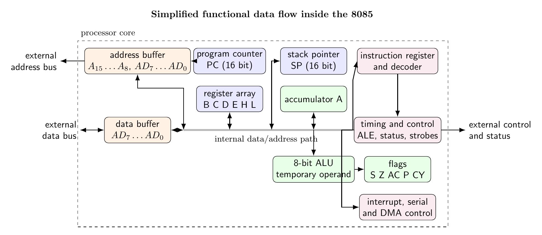
Internally, the program counter supplies the address of the next instruction byte. Address buffers drive the external address interface. An opcode read from memory passes through the data buffer into the instruction register, where the decoder and timing/control unit determine the required micro-operations and bus cycles.
The programmer-visible data path includes accumulator A, six general registers B, C, D, E, H, and L, the flag register, the stack pointer, and the program counter. An internal temporary register participates in ALU operations but is not directly addressable. The ALU takes an accumulator operand and another selected operand, produces an 8-bit result, and updates only the flags defined for that instruction.
Fetch, decode and execute
For an opcode fetch at address $P$, the sequence is conceptually:
- PC places $P$ on the address path;
ALEmarks the low-address phase. - The timing unit requests a memory read with opcode-fetch status.
- The addressed byte enters the instruction register, and PC advances modulo $2^{16}$.
- The decoder interprets the opcode and selects subsequent internal transfers or external cycles.
- Execution writes a result to a register, memory, PC, SP, or an I/O device as specified.
For MVI A,5AH, decode of 3EH demands one more program-memory read, and the returned byte is loaded into A. For LDA 2500H, two further reads obtain the low and high address bytes; after the effective address is assembled, another read obtains the data. For ADD B, B is selected internally and no data-memory cycle is required. Thus one common control mechanism generates different sequences from the opcode and addressing mode.
Bus observability does not expose every internal action. A logic analyzer can see addresses, data, ALE, status, and strobes, but register selection and ALU carries are internal. Correct debugging combines external cycle traces with the documented instruction state changes.
Preparation questions
- Explain how an 8-bit multiplexed group lets the 8085 provide a 16-bit address and an 8-bit data interface in forty pins.
- Design the logical connections of an address latch using
AD7–AD0andALE, and state what the latch output represents after the address phase. - Decode the combinations of
IO/M,S1,S0, active-lowRD, and active-lowWRfor memory and I/O transfers. - Distinguish a T-state, a machine cycle, an instruction cycle, and a wait state.
- Compare
READYwith theHOLD/HLDAhandshake and give one application for each. - List the hardware interrupts in priority order and distinguish vectored, maskable, edge-triggered, and level-sensitive behavior.
- Trace the external and internal steps required by
MVI A,5AH,ADD B, andLDA 2500H.


Discussion