

03 Jun 2025
AC Differential Analysis, Balanced Output and CMRR
Odd- and even-mode small-signal analysis of the dual-input differential pair, differential and common-mode gains, CMRR, mismatch and frequency dependence.
Small-signal analysis separates the two independent ways in which a symmetrical differential amplifier can be excited. The differential or odd-mode input changes the two base voltages in opposite directions; the common or even-mode input changes them together. Symmetry then reduces the full two-transistor circuit to a half-circuit for each mode.
Write the input voltages as
\[v_1=v_{cm}+\frac{v_d}{2}, \qquad v_2=v_{cm}-\frac{v_d}{2},\]where
\[v_d=v_1-v_2, \qquad v_{cm}=\frac{v_1+v_2}{2}.\]Incremental voltages are measured from the DC operating point, supply rails are AC grounds, transistor junction capacitances are initially neglected, and both BJTs are matched and forward active. At quiescent collector current $I_C$,
\[g_m=\frac{I_C}{V_T}, \qquad r_\pi=\frac{\beta}{g_m}, \qquad r_e\simeq\frac{1}{g_m}.\]The output signs are $v_{od}=v_{o1}-v_{o2}$ and $A_{vd}=v_{od}/v_d$ unless a single-ended output is explicitly identified.
Differential excitation and the virtual-ground plane
Set $v_{cm}=0$, so $v_1=+v_d/2$ and $v_2=-v_d/2$. The circuit and its excitation are antisymmetric about the vertical centre plane. The incremental emitter currents are equal and opposite, so their sum is zero. No signal current enters the tail element, even if its resistance is finite. The common-emitter node is therefore a virtual AC ground for a perfectly matched pair.
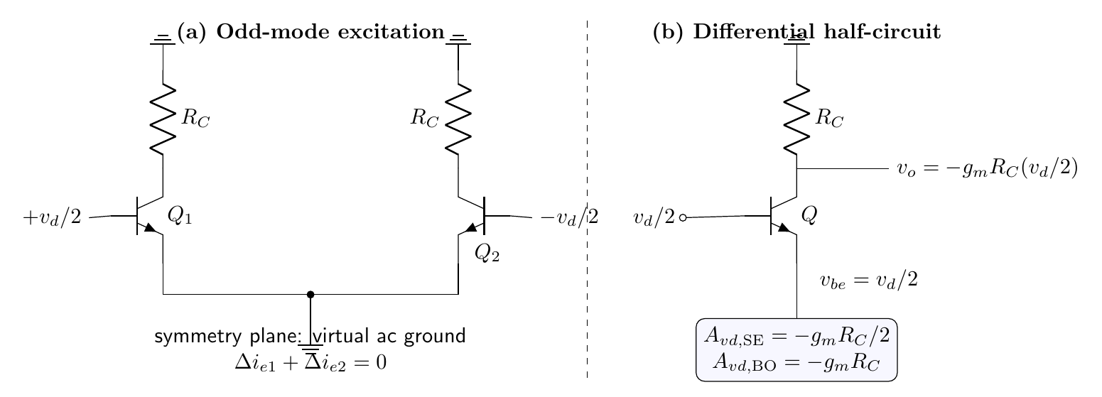
Consequently
\[v_{be1}=+\frac{v_d}{2}, \qquad v_{be2}=-\frac{v_d}{2},\]and
\[i_{c1}=g_m\frac{v_d}{2}, \qquad i_{c2}=-g_m\frac{v_d}{2}.\]For equal collector loads $R_C$ and negligible transistor output conductance,
\[v_{o1}=-i_{c1}R_C=-\frac{g_mR_C}{2}v_d,\] \[v_{o2}=-i_{c2}R_C=+\frac{g_mR_C}{2}v_d.\]The single-ended differential gain at collector 1 and the balanced-output gain are therefore
\[\boxed{A_{vd,SE}=-\frac{g_mR_C}{2}}, \qquad \boxed{A_{vd,BO}=\frac{v_{o1}-v_{o2}}{v_d}=-g_mR_C}.\]The balanced output is twice either single-ended signal because it subtracts two outputs of equal magnitude and opposite phase. If transistor output resistance $r_o$ and an external load are included, $R_C$ is replaced by the effective collector load. For a differential load $R_L$ connected between collectors, each half-circuit sees $R_L/2$, giving
\[A_{vd,BO}=-g_m\left(R_C\parallel r_o\parallel\frac{R_L}{2}\right).\]Operation with only one input driven
The common laboratory connection $v_1=v_i$, $v_2=0$ is not a pure odd-mode excitation. Its decomposition is
\[v_d=v_i, \qquad v_{cm}=\frac{v_i}{2}.\]For collector 1, superposition gives
\[v_{o1}=A_{vd,SE}v_i+A_{vcm,SE}\frac{v_i}{2},\]while collector 2 gives
\[v_{o2}=-A_{vd,SE}v_i+A_{vcm,SE}\frac{v_i}{2}.\]When $\lvert A_{vcm}\rvert\ll\lvert A_{vd}\rvert$, collector 1 is an inverting output and collector 2 is a non-inverting output relative to the driven base. Subtracting the collectors removes the common-mode contribution exactly for matched branches:
\[v_{od}=v_{o1}-v_{o2}=2A_{vd,SE}v_i=A_{vd,BO}v_i.\]This result explains why the same physical pair supports inverting, non-inverting, dual-input and balanced-output use; the labels refer to the chosen input and output terminals, not to different transistor circuits.
The differential input resistance measured between the two bases is
\[\boxed{R_{id}=2r_\pi}\]for the un-degenerated pair. If each emitter contains a resistor $R_E$, then approximately
\[R_{id}=2\left[r_\pi+(\beta+1)R_E\right],\]while the balanced gain becomes approximately $-R_C/(r_e+R_E)$.
Finite transistor output resistance and loading
The preceding gain expressions neglect the Early effect. In the hybrid-$\pi$ model, each collector has an output resistance $r_o$ to its emitter. The differential symmetry plane remains an AC ground, so the effective collector load in each half-circuit is
\[R_{Ld}=R_C\parallel r_o\parallel R_{in,next}.\]Accordingly,
\[A_{vd,SE}\simeq-\frac{g_mR_{Ld}}{2}, \qquad A_{vd,BO}\simeq-g_mR_{Ld},\]provided both sides have equal loads. If a load $R_L$ is connected directly between the collectors, odd-mode symmetry puts its midpoint at AC ground; each half then sees $R_L/2$. This factor of two is frequently missed when a balanced load is reduced to a half-circuit.
Finite $r_o$ also couples collector-voltage changes back into collector currents. The simple replacement $R_C\mapsto R_C\parallel r_o$ is the leading-order result when the emitter node remains fixed. A complete hybrid-$\pi$ solution is required when collector-base feedback, unequal $r_o$ values or a finite impedance in the emitter path destroys that separation.
Common-mode excitation
For $v_1=v_2=v_{cm}$, both sides carry equal, in-phase incremental currents. The centre plane is now an open symmetry plane rather than a ground. Let the small-signal tail resistance be $R_{EE}$; for a transistor current source it is the source’s output resistance, not its DC setting resistance.
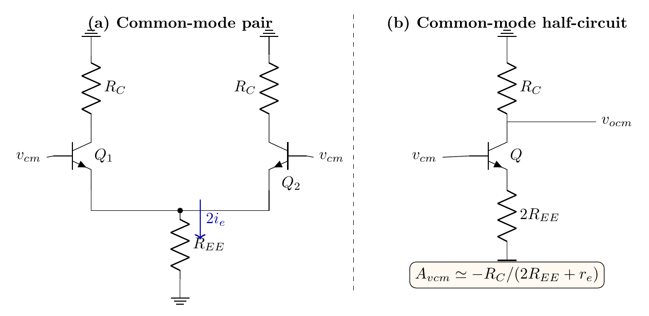
In the transistor T model, each emitter current is
\[i_e=\frac{v_{cm}}{r_e+2R_{EE}}.\]For $\alpha\simeq1$, $i_c\simeq i_e$ and the single-ended common-mode gain is
\[\boxed{ A_{vcm,SE}=\frac{v_{ocm}}{v_{cm}} \simeq-\frac{R_C}{r_e+2R_{EE}} }.\]When $R_{EE}\gg r_e$,
\[A_{vcm,SE}\simeq-\frac{R_C}{2R_{EE}}.\]The same result can be obtained without a half-circuit. If the common-emitter voltage is $v_e$, the two branch currents are $(v_{cm}-v_e)/r_e$, and KCL gives
\[\frac{v_e}{R_{EE}}= 2\frac{v_{cm}-v_e}{r_e}.\]Solving,
\[v_e=\frac{2R_{EE}}{2R_{EE}+r_e}v_{cm},\]so only the small residual
\[v_{be}=v_{cm}-v_e =\frac{r_e}{2R_{EE}+r_e}v_{cm}\]acts on either transistor. A high-resistance tail source therefore causes the emitter node to follow the common-mode input, leaving nearly constant $v_{BE}$ and collector current.
An ideal tail-current source has $R_{EE}\to\infty$ and therefore zero common-mode gain. A practical source has finite output resistance because of the Early effect, so common-mode motion changes the tail current slightly.
The common-mode input resistance seen at either base is much larger than $r_\pi$. A base-current increment $i_b$ produces emitter current $(\beta+1)i_b$, and both emitter currents flow through the tail resistance. Each common-mode half-circuit therefore gives approximately
\[\boxed{R_{ic,\mathrm{per\ input}} =r_\pi+(\beta+1)(2R_{EE})}.\]This large resistance assumes that both inputs are driven together. Driving only one base is neither a pure differential nor a pure common-mode experiment; it is the superposition of both and must be decomposed using $v_d$ and $v_{cm}$.
For exactly matched collector branches the two common-mode output voltages are equal. Their balanced difference is zero even when each single-ended common-mode gain is nonzero:
\[A_{vcm,BO}=\frac{v_{o1}-v_{o2}}{v_{cm}}=0.\]Thus a quoted CMRR must identify whether the output is single-ended or balanced and whether mismatch is included.
Common-mode rejection ratio
For a single-ended output,
\[\mathrm{CMRR}=\left\lvert\frac{A_{vd,SE}}{A_{vcm,SE}}\right\rvert =\frac{g_m(r_e+2R_{EE})}{2}.\]Since $g_mr_e\simeq1$,
\[\boxed{\mathrm{CMRR}\simeq g_mR_{EE}} \qquad (g_mR_{EE}\gg1).\]In decibels,
\[\boxed{\mathrm{CMRR}_{\mathrm{dB}} =20\log_{10}\!\left\lvert\frac{A_{vd}}{A_{vcm}}\right\rvert}.\]CMRR is a voltage-gain ratio and therefore uses $20\log_{10}$, not $10\log_{10}$. It is improved by increasing the tail-source output resistance, increasing transistor transconductance, matching the two sides, and taking a balanced output.
Mismatch-limited balanced rejection
Let $R_{C1}=R_C+\Delta R_C/2$ and $R_{C2}=R_C-\Delta R_C/2$. Under common-mode excitation both collector currents change by
\[i_c\simeq\frac{v_{cm}}{2R_{EE}+r_e}.\]Their output difference is no longer zero:
\[v_{od,cm}=-i_c(R_{C1}-R_{C2}),\]so
\[\boxed{A_{vcm,BO}\simeq -\frac{\Delta R_C}{2R_{EE}+r_e}}.\]Transconductance mismatch, unequal output resistances and unequal parasitic capacitances generate similar residual terms. In an integrated circuit, common-centroid geometry and close thermal coupling are used because ratio matching is more accurate than absolute component accuracy.
Frequency dependence
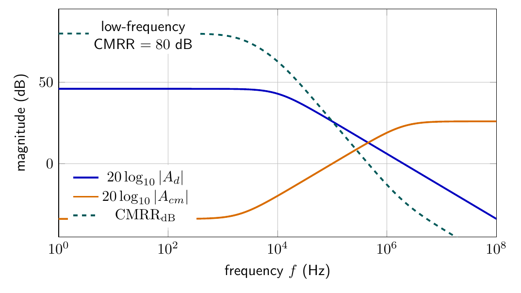
At higher frequency, collector-base capacitance and the voltage-amplifier load reduce $A_d$. Parasitic capacitance at the tail-source output can also reduce its impedance, increasing $A_{cm}$. A simple illustrative representation is
\[A_d(j\omega)=\frac{A_{d0}}{1+j\omega/\omega_d},\]while the common-mode path generally has different poles and zeros. Consequently
\[\mathrm{CMRR}(j\omega)=\frac{A_d(j\omega)}{A_{cm}(j\omega)}\]usually decreases before the differential gain reaches its unity-gain frequency.
If the tail source has an output capacitance $C_T$, its impedance can be approximated by
\[Z_T(j\omega)=\frac{r_{o,T}}{1+j\omega r_{o,T}C_T}.\]Substitution into the even-mode result gives
\[A_{vcm}(j\omega)\simeq -\frac{R_C}{r_e+2Z_T(j\omega)}.\]Above $1/(2\pi r_{o,T}C_T)$, the magnitude of $Z_T$ falls, so common-mode gain can rise even while differential gain is beginning to fall. Device data therefore specify CMRR versus frequency rather than only its DC value.
Worked small-signal calculation
For $I_C=0.500\ \mathrm{mA}$ per transistor, $R_C=10.0\ \mathrm{k\Omega}$, $R_{EE}=100\ \mathrm{k\Omega}$, $\beta=150$ and $T=300\ \mathrm K$,
\[g_m=\frac{0.500\ \mathrm{mA}}{25.85\ \mathrm{mV}} =19.34\ \mathrm{mS},\] \[r_e=51.7\ \Omega, \qquad r_\pi=7.76\ \mathrm{k\Omega}.\]Therefore
\[A_{vd,SE}=-96.7, \qquad A_{vd,BO}=-193.4,\]and
\[A_{vcm,SE}=-\frac{10.0\ \mathrm{k\Omega}} {200\ \mathrm{k\Omega}+51.7\ \Omega} =-0.04999.\]The single-ended CMRR is
\[\mathrm{CMRR}=\frac{96.7}{0.04999}=1.934\times10^3,\] \[\mathrm{CMRR}_{\mathrm{dB}}=65.7\ \mathrm{dB}.\]To obtain approximately $90\ \mathrm{dB}$ at the same $g_m$, the required tail resistance follows from $\mathrm{CMRR}\simeq g_mR_{EE}$:
\[R_{EE}\simeq\frac{10^{90/20}}{19.34\ \mathrm{mS}} =1.64\ \mathrm{M\Omega}.\]This large value explains the use of transistor current sources rather than ordinary tail resistors in operational-amplifier input stages.
Preparation questions
- Use odd-mode symmetry to derive the single-ended and balanced differential gains of a matched BJT differential pair.
- Show why the finite tail resistance is absent from ideal differential-mode gain but controls common-mode gain.
- Derive the common-mode half-circuit and prove that each transistor sees $2R_{EE}$.
- Define CMRR for both single-ended and balanced outputs, and explain why a perfectly symmetrical balanced output gives zero common-mode response.
- A pair has $I_C=0.25\ \mathrm{mA}$, $R_C=22\ \mathrm{k\Omega}$ and $R_{EE}=500\ \mathrm{k\Omega}$. Calculate $A_{vd,SE}$, $A_{vcm,SE}$ and CMRR at $300\ \mathrm K$.
- Derive the residual balanced common-mode gain caused by a difference $\Delta R_C$ between the collector loads.


Discussion