

05 Jun 2025
Constant-Current Sources, Active Loads and Bias-Level Translation
BJT current mirrors, finite-beta and Early-effect errors, differential active loads, high-gain conversion and DC level translation in operational amplifiers.
Operational amplifiers require nearly constant currents to establish transistor operating points, high-resistance active loads to obtain large voltage gain, and level translators to place the amplified signal at the correct DC voltage for the output stage. These functions are closely related: a transistor biased as a current source has a large incremental output resistance and can therefore serve as both a bias element and an active load.
Conventional current directions and SI units are used. NPN devices are assumed forward active unless a compliance limit is being discussed. For small-signal calculations, DC supplies are AC grounds and $r_o=V_A/I_C$ represents the Early-effect output resistance.
Ideal and practical constant-current elements
An ideal current source delivers a specified current independently of its terminal voltage. Its small-signal output resistance is infinite:
\[r_{out}=\left(\frac{\partial i_o}{\partial v_o}\right)^{-1}\to\infty.\]A practical source maintains approximately constant current only over a compliance range. If its transistor enters saturation at low output voltage or approaches breakdown at high output voltage, regulation is lost. Within the active region, Early effect gives
\[I_C\simeq I_{C0}\left(1+\frac{V_{CE}}{V_A}\right), \qquad r_o\simeq\frac{V_A}{I_C}.\]Thus a large Early voltage and a small bias current produce a large source resistance. Cascoded sources increase resistance further by holding the current-setting transistor’s $V_{CE}$ nearly constant, but they consume additional voltage headroom.
Simple BJT current mirror
In the elementary NPN mirror, $Q_1$ is diode-connected by joining its collector to its base. The resistor establishes a reference current and forces the same $V_{BE}$ on matched output transistor $Q_2$.
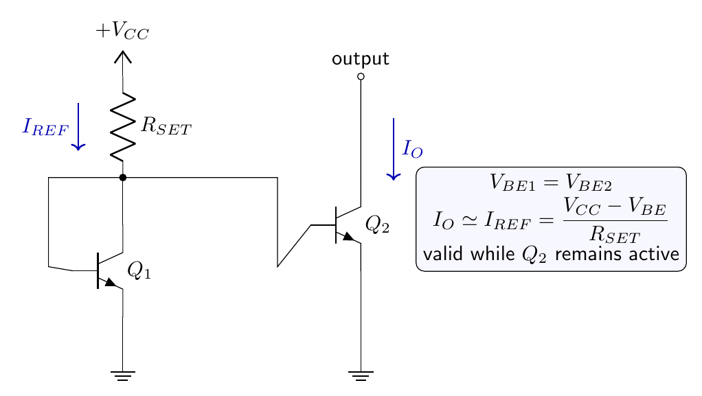
Neglecting base currents and Early effect,
\[I_{REF}\simeq\frac{V_{CC}-V_{BE}}{R_{SET}}, \qquad I_O\simeq I_{REF}.\]With equal finite current gain $\beta$, Kirchhoff’s law at the common base node is
\[I_{REF}=I_{C1}+I_{B1}+I_{B2}.\]For matched collector currents $I_{C1}=I_{C2}=I_O$ and $I_B=I_O/\beta$,
\[\boxed{I_O=\frac{I_{REF}}{1+2/\beta}}.\]The relative error is approximately $-2/\beta$ when $\beta\gg1$. A Wilson mirror uses feedback to reduce base-current error and raise output resistance; a cascode mirror chiefly suppresses the dependence on output voltage. Neither improvement removes the need for adequate compliance voltage.
The reference transistor usually has $V_{CE1}=V_{BE}$, whereas the output transistor has $V_{CE2}=V_O$. With Early effect,
\[\frac{I_O}{I_{C1}} \simeq \frac{1+V_O/V_A}{1+V_{BE}/V_A}.\]This systematic error can exceed the finite-$\beta$ error if the collector voltages differ appreciably. Precision integrated mirrors use equal device geometry, thermal proximity, suitable emitter-area ratios and circuit arrangements that equalize collector voltages.
If the emitter area of $Q_2$ is $m$ times that of $Q_1$ and their current densities are equal, the ideal mirror ratio becomes
\[I_O=mI_{C1}.\]Finite base currents now give
\[I_{REF}=I_{C1}\left[1+\frac{1+m}{\beta}\right],\]and hence
\[I_O=\frac{mI_{REF}}{1+(1+m)/\beta}.\]Area scaling is preferable to using unmatched emitter resistors when an accurate integer current ratio is required on one chip. Emitter resistors are nevertheless useful for degeneration: they reduce sensitivity to $V_{BE}$ mismatch and improve thermal stability, while consuming compliance voltage.
For equal device areas, a small base-emitter mismatch $\Delta V_{BE}$ produces approximately
\[\frac{\Delta I}{I}\simeq\frac{\Delta V_{BE}}{V_T}.\]Even $1\ \mathrm{mV}$ corresponds to nearly four percent at room temperature. Monolithic mirrors are effective because adjacent devices have well-matched junctions and nearly the same temperature; separated discrete transistors require careful thermal coupling.
Current source as the differential-pair tail
A resistor connected from the joined emitters to a negative supply fixes current only approximately:
\[I_T\simeq\frac{V_E+V_{EE}}{R_{EE}}.\]Common-mode motion changes $V_E$ and therefore changes $I_T$. Replacing the resistor by a transistor current sink makes the DC current reproducible from a reference and gives a much larger small-signal tail resistance. Because
\[A_{vcm}\simeq-\frac{R_C}{2r_{o,T}},\]increasing the tail-source output resistance directly improves common-mode rejection. The source must remain active throughout the permitted input common-mode range; otherwise CMRR and differential gain collapse.
Current-mirror active load
Resistor collector loads occupy substantial chip area and their resistance cannot be made arbitrarily large without consuming DC voltage. A PNP current mirror can replace the two collector resistors of an NPN differential pair. The mirror provides a large incremental load resistance and converts the two-ended collector-current signal into a single-ended current.
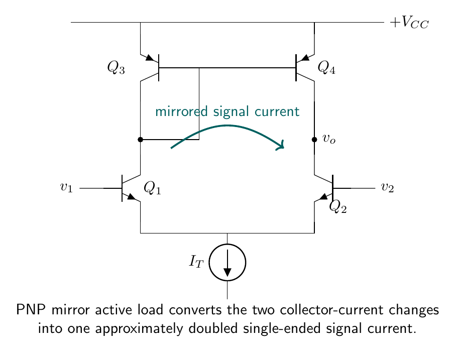
Let $v_d=v_1-v_2$, and neglect mirror error. Around the balanced operating point,
\[\Delta i_{C1}=+\frac{g_m v_d}{2}, \qquad \Delta i_{C2}=-\frac{g_m v_d}{2}.\]The PNP mirror reproduces the left-branch increment as an additional source-current increment at the output. At the right output node, the mirror source current increases by $g_mv_d/2$ while the NPN sink current decreases by the same amount. The net current available to charge the output node is therefore
\[\boxed{\Delta i_o\simeq g_m v_d}.\]For the output shown in the figure, positive $v_d$ raises $v_o$, so the low-frequency gain is
\[\boxed{A_v\simeq+g_mR_{out}},\]where, to first order,
\[R_{out}\simeq r_{o,n}\parallel r_{o,p}\parallel R_{in,next}.\]The polarity would reverse if the output were taken at the opposite collector or if the input labels were interchanged. The gain is large because $R_{out}$ can be tens or hundreds of kilohms without a physical resistor of that value.
The mirror does not exactly double the signal at high frequency. Its diode-connected transistor has finite input resistance and capacitance; PNP and NPN transition frequencies may differ; and mismatch converts common-mode signal to differential output. The high-resistance output node is also an important pole of the amplifier.
Bias-level translation
Successive high-gain stages can place the signal on an unsuitable DC level. For example, the collector of an NPN voltage-amplifier transistor may rest near the positive supply, whereas a complementary output stage requires its input near zero volts. A level translator changes the quiescent voltage while preserving the incremental waveform.
An emitter follower biased by a current sink is a basic downward translator. Its quiescent relation is
\[\boxed{V_{OQ}\simeq V_{IQ}-V_{BE}}.\]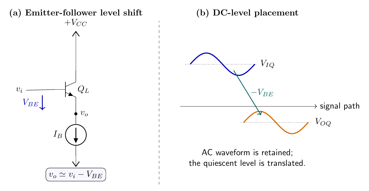
Using the emitter small-signal resistance $r_e$ and the effective load $R_L$ at the emitter,
\[A_v\simeq\frac{R_L}{R_L+r_e},\]which is close to unity when $R_L\gg r_e$. The output resistance is low compared with that of the preceding collector node, so the follower also provides buffering. Two forward-biased junctions give approximately $2V_{BE}$ translation. A $V_{BE}$ multiplier with $R_1$ from collector to base and $R_2$ from base to emitter provides the adjustable voltage
\[V_{shift}\simeq V_{BE}\left(1+\frac{R_1}{R_2}\right),\]and is widely used to establish class-AB output-stage bias.
The translation is not an ideal fixed voltage. $V_{BE}$ depends logarithmically on current and decreases with temperature by roughly $2\ \mathrm{mV/K}$ at constant current. Bias networks are therefore thermally coupled to the output devices when their purpose includes controlling quiescent class-AB current.
The translator must also meet a signal-swing condition. Its current sink requires a minimum voltage and the follower collector must remain above its emitter by more than $V_{CE(sat)}$. A quiescent shift that is correct algebraically can therefore fail near one signal peak. Internal op-amp design allocates voltage headroom among the gain transistor, translator and output driver for the full specified supply range.
Numerical design example
Take $V_{CC}=12.0\ \mathrm V$, $R_{SET}=10.0\ \mathrm{k\Omega}$, $V_{BE}=0.70\ \mathrm V$, $\beta=100$ and $V_A=100\ \mathrm V$. The mirror reference current is
\[I_{REF}=\frac{12.0-0.70}{10.0\ \mathrm{k\Omega}} =1.130\ \mathrm{mA}.\]Base-current loading gives
\[I_O=\frac{1.130\ \mathrm{mA}}{1+2/100} =1.108\ \mathrm{mA}.\]If $V_O=5.0\ \mathrm V$ while $V_{CE1}=0.70\ \mathrm V$, a first-order Early-effect correction multiplies this by
\[\frac{1+5/100}{1+0.70/100}=1.0427,\]giving $I_O\simeq1.155\ \mathrm{mA}$. The two nonidealities partly cancel in this particular numerical case; this cancellation is accidental and changes with output voltage.
For a mirror-loaded differential pair with $I_C=0.500\ \mathrm{mA}$, $V_{A,n}=100\ \mathrm V$ and $V_{A,p}=80\ \mathrm V$,
\[g_m=19.34\ \mathrm{mS}, \quad r_{o,n}=200\ \mathrm{k\Omega}, \quad r_{o,p}=160\ \mathrm{k\Omega},\] \[R_{out}=88.9\ \mathrm{k\Omega}, \qquad A_v\simeq +(19.34\ \mathrm{mS})(88.9\ \mathrm{k\Omega}) =+1.72\times10^3.\]This is an intrinsic low-frequency estimate. Loading by the following stage and frequency compensation reduce the realized stage gain.
Preparation questions
- Derive the finite-$\beta$ output current of a two-transistor BJT mirror and state every approximation.
- Explain the compliance limitation and derive the small-signal output resistance associated with Early effect.
- Show how a transistor tail-current source improves the CMRR of a differential amplifier.
- For a mirror-loaded differential pair, prove that the two collector-current increments combine to give an effective transconductance of magnitude $g_m$.
- Calculate the finite-$\beta$ and Early-effect errors for $V_{CC}=15\ \mathrm V$, $R_{SET}=15\ \mathrm{k\Omega}$, $\beta=80$, $V_A=120\ \mathrm V$ and $V_O=8\ \mathrm V$.
- Derive the DC shift and small-signal gain of a current-biased emitter-follower level translator, including a finite emitter load.


Discussion