

01 Jun 2025
Differential Amplifier: Circuit Configuration and DC Analysis
Matched BJT differential-pair topology, quiescent bias, large-signal current steering, output levels, compliance and a complete numerical design calculation.
A differential amplifier responds primarily to the difference between two input voltages. It is the input stage of an operational amplifier because it permits a direct comparison of the signal and the feedback voltage, rejects disturbances common to both input terminals, and provides a symmetrical bias point from which large voltage gain can be developed.
The analysis uses matched NPN transistors, SI units and the sign convention
\[v_d\equiv v_1-v_2, \qquad v_{od}\equiv v_{o1}-v_{o2}.\]The tail-current arrow denotes conventional current drawn from the joined emitters. Unless stated otherwise, both transistors operate in forward active mode, their temperatures are equal, the Early effect is neglected, and the tail source has infinite small-signal resistance.
Basic dual-input, balanced-output circuit
Two nominally identical transistors $Q_1$ and $Q_2$ share a common emitter node. Equal collector resistors $R_C$ connect the collectors to $+V_{CC}$, while a current sink fixes the total emitter current at $I_T$. Both collectors are available, so the circuit has dual inputs and balanced outputs.
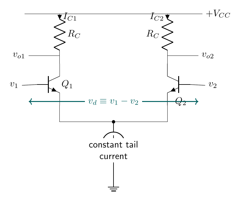
Kirchhoff’s current law at the joined emitters gives
\[I_{E1}+I_{E2}=I_T.\]For high current gain $\beta$, $I_C\simeq I_E$ and hence $I_{C1}+I_{C2}\simeq I_T$. If base-current error is retained and both transistors have the same $\beta$,
\[I_{C1}+I_{C2}=\alpha I_T, \qquad \alpha=\frac{\beta}{\beta+1}.\]The collector voltages are
\[v_{o1}=V_{CC}-R_C I_{C1}, \qquad v_{o2}=V_{CC}-R_C I_{C2},\]so that the balanced output is
\[\boxed{v_{od}=-R_C(I_{C1}-I_{C2})}.\]This polarity follows directly from the stated sign convention: greater $v_1$ produces greater $I_{C1}$ and therefore a smaller $v_{o1}$.
Quiescent DC state
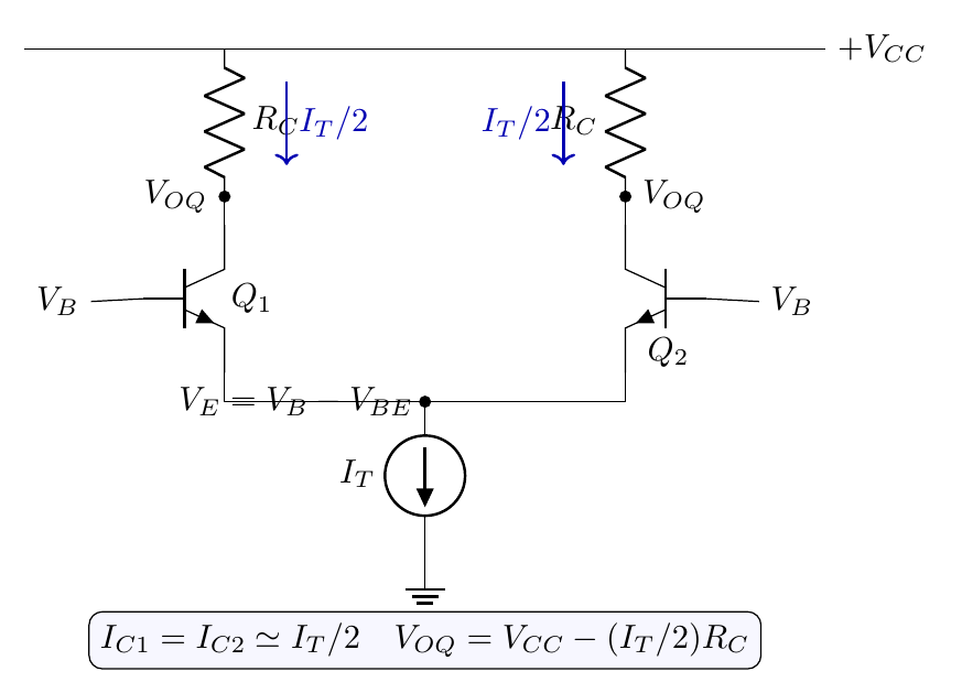
Set $v_1=v_2=V_B$. Matched devices then have the same base-emitter voltage, so symmetry requires
\[I_{E1}=I_{E2}=\frac{I_T}{2}, \qquad I_{C1}=I_{C2}=\frac{\alpha I_T}{2}.\]The emitter and collector quiescent voltages are
\[V_E=V_B-V_{BEQ}, \qquad \boxed{V_{OQ}=V_{CC}-\frac{\alpha I_T R_C}{2}}.\]Consequently $V_{od,Q}=0$, although each collector can sit at a substantial nonzero DC potential. A balanced output rejects this common DC level.
For an NPN transistor to remain in forward-active operation, its collector-base junction must not become forward biased. At the boundary of saturation,
\[V_C=V_B=V_E+V_{BE}.\]Thus a design with a specified minimum collector-base headroom $V_{CB,\min}\ge0$ must satisfy $V_C\ge V_B+V_{CB,\min}$. The commonly quoted $V_{CE(sat)}$ is the collector-emitter voltage in an already saturated transistor; it is not the forward-active boundary. During complete steering, one collector can carry almost $\alpha I_T$, so a conservative lower collector voltage is
\[V_{C,\min}=V_{CC}-\alpha I_T R_C.\]If $V_{B,\max}$ is the largest base voltage permitted while that branch carries the full current, the design must satisfy
\[\boxed{V_{CC}-\alpha I_T R_C \ge V_{B,\max}+V_{CB,\min}}.\]It must also provide adequate voltage across the tail source. A transistor current sink ceases to behave as a high-resistance source if its compliance voltage becomes too small. Thus the common-emitter voltage cannot be chosen from the transistor pair alone; it must also be compatible with the negative supply and the current-source implementation.
Resistive tail bias and input common-mode range
If the ideal sink is replaced by a resistor $R_{EE}$ connected to a negative rail $-V_{EE}$, equal inputs give
\[I_T=\frac{V_E+V_{EE}}{R_{EE}} =\frac{V_B-V_{BEQ}+V_{EE}}{R_{EE}}.\]This expression must be solved consistently because $V_{BEQ}$ itself depends logarithmically on current. If $V_{BEQ}$ is first estimated, a single update with
\[V_{BEQ}=V_T\ln\!\left(\frac{\alpha I_T/2}{I_S}\right)\]is normally sufficient for hand design. Unlike an ideal current source, the resistor permits the tail current to change with common-mode input. A common-mode increase $\Delta V_{cm}$ produces approximately
\[\Delta I_T\simeq\frac{\Delta V_{cm}}{R_{EE}+r_e/2},\]where $r_e/2$ is the parallel incremental emitter resistance of the two devices. This dependence is the origin of finite common-mode gain for a resistively biased pair.
The DC common-mode range has both upper and lower limits. At high $V_{cm}$, the emitter voltage rises and each collector must remain at or above its base by the chosen collector-base margin:
\[V_C-V_{cm}\ge V_{CB,\min}.\]For the balanced state this gives the approximate upper bound
\[\boxed{V_{cm,\max}\le V_{CC}-\frac{\alpha I_TR_C}{2}-V_{CB,\min}}.\]At low $V_{cm}$, a transistor tail sink must retain its own compliance voltage $V_{CS,\min}$. If the negative rail is $-V_{EE}$,
\[V_{cm,\min}>-V_{EE}+V_{CS,\min}+V_{BEQ}.\]These inequalities are approximate because the tail current, $V_{BE}$ and collector voltage change together near the limits. They nevertheless identify the two distinct failure mechanisms: saturation of an input transistor at the upper end and loss of tail-source regulation at the lower end.
Exact large-signal current steering
For matched BJTs at a common temperature,
\[I_{C1}=I_S e^{v_{BE1}/V_T}, \qquad I_{C2}=I_S e^{v_{BE2}/V_T},\]where $V_T=k_BT/q$. Since the emitters are joined,
\[v_{BE1}-v_{BE2}=v_1-v_2=v_d,\]and therefore
\[\frac{I_{C1}}{I_{C2}}=e^{v_d/V_T}.\]Combining this ratio with $I_{C1}+I_{C2}=\alpha I_T$ yields the exact ideal-tail-source relations
\[\boxed{ I_{C1}=\frac{\alpha I_T}{1+e^{-v_d/V_T}}, \qquad I_{C2}=\frac{\alpha I_T}{1+e^{v_d/V_T}} }.\]Their difference is
\[I_{C1}-I_{C2} =\alpha I_T\tanh\!\left(\frac{v_d}{2V_T}\right),\]and hence
\[\boxed{ v_{od}=-\alpha I_T R_C \tanh\!\left(\frac{v_d}{2V_T}\right) }.\]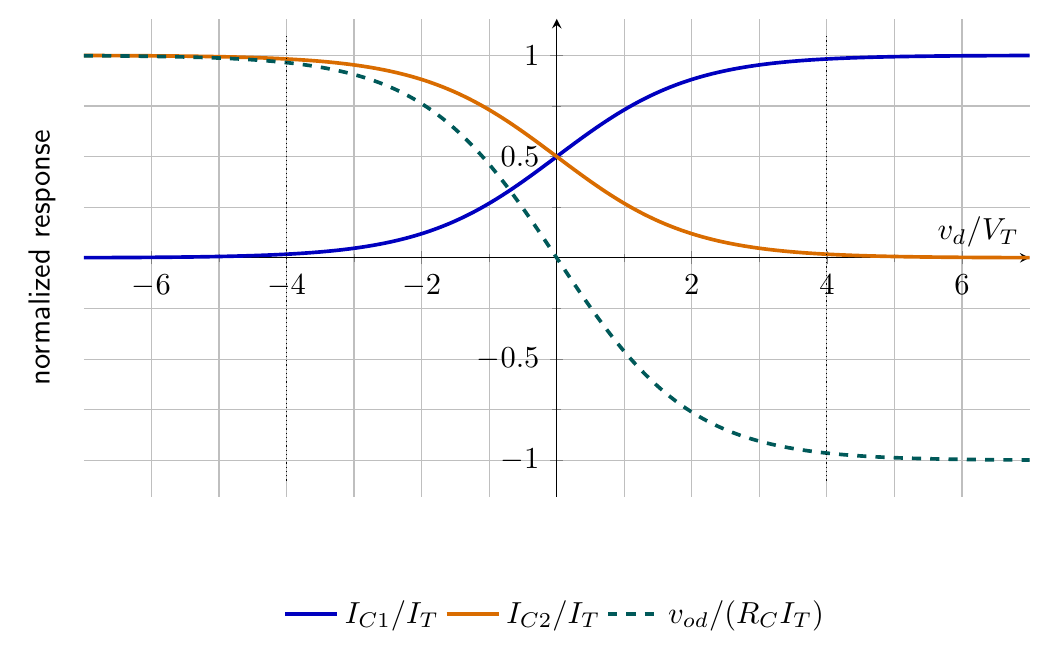
At room temperature $V_T\simeq25.85\ \mathrm{mV}$. Thus a differential input of only a few thermal voltages nearly switches the complete tail current. This is why an uncompensated differential pair is linear only for small differential inputs.
Linear differential range and DC transconductance
For $\lvert v_d\rvert\ll2V_T$, $\tanh x\simeq x-x^3/3+\cdots$. The balanced output becomes
\[v_{od}\simeq -\frac{\alpha I_T R_C}{2V_T}v_d +\frac{\alpha I_T R_C}{24V_T^3}v_d^3+\cdots.\]Since the quiescent collector current is $I_{CQ}=\alpha I_T/2$, the transistor transconductance is
\[g_m=\frac{I_{CQ}}{V_T}=\frac{\alpha I_T}{2V_T}.\]The small-input balanced-output gain is consequently
\[\boxed{A_{vd,BO}\equiv \left.\frac{dv_{od}}{dv_d}\right\rvert_{v_d=0} =-g_mR_C}.\]For a single-ended output at collector 1, $\Delta I_{C1}=g_m v_d/2$ and
\[A_{vd,SE}=\frac{\Delta v_{o1}}{v_d} =-\frac{g_mR_C}{2}.\]The cubic-to-linear magnitude ratio is approximately $v_d^2/(12V_T^2)$. Requiring it to be less than one percent gives $\lvert v_d\rvert<\sqrt{0.12}V_T\simeq9\ \mathrm{mV}$ at $300\ \mathrm K$. Emitter-degeneration resistors can enlarge the linear range, at the cost of reduced gain.
Worked DC and transfer calculation
Let $V_{CC}=12.0\ \mathrm V$, $I_T=2.00\ \mathrm{mA}$, $R_C=4.70\ \mathrm{k\Omega}$, $\beta=150$, $V_B=0$, $V_{BEQ}=0.70\ \mathrm V$ and $T=300\ \mathrm K$. Then
\[\alpha=\frac{150}{151}=0.99338, \quad I_{CQ}=\frac{\alpha I_T}{2}=0.9934\ \mathrm{mA},\] \[V_E=-0.70\ \mathrm V, \qquad V_{OQ}=12-(0.9934\ \mathrm{mA})(4.70\ \mathrm{k\Omega}) =7.331\ \mathrm V.\]For $v_d=+10.0\ \mathrm{mV}$,
\[\frac{v_d}{V_T}=0.38685,\] \[I_{C1}=1.1832\ \mathrm{mA}, \qquad I_{C2}=0.8036\ \mathrm{mA},\]and
\[v_{od}=-4.70\ \mathrm{k\Omega}(1.1832-0.8036)\ \mathrm{mA} =-1.784\ \mathrm V.\]The linear estimate is
\[-g_mR_Cv_d =-\frac{0.9934\ \mathrm{mA}}{25.85\ \mathrm{mV}} (4.70\ \mathrm{k\Omega})(10.0\ \mathrm{mV}) =-1.806\ \mathrm V,\]which differs by about one percent. With the current fully steered, the lowest collector voltage is
\[V_{C,\min}=12-(1.9868\ \mathrm{mA})(4.70\ \mathrm{k\Omega}) =2.662\ \mathrm V.\]The strict forward-active requirement under full steering is therefore
\[V_{B,\max}<2.662\ \mathrm V\]when the limiting value $V_{CB,\min}=0$ is used. Inputs near the stated $0\ \mathrm V$ bias consequently retain ample collector-base headroom. At balance, the zero-margin common-mode upper boundary is $V_{cm,\max}=V_{OQ}=7.331\ \mathrm V$; a practical design subtracts its required positive $V_{CB,\min}$.
DC load line and device dissipation
For either collector branch the resistor imposes the load-line relation
\[V_C=V_{CC}-I_CR_C.\]Together with the nearly fixed emitter voltage, this gives
\[V_{CE}=V_{CC}-I_CR_C-V_E.\]The transistor dissipation along the load line is approximately
\[P_Q=I_CV_{CE} =I_C(V_{CC}-V_E-I_CR_C).\]It is a quadratic function of current and reaches its load-line maximum at
\[I_C=\frac{V_{CC}-V_E}{2R_C},\]if that current lies within the steering interval $0\le I_C\le\alpha I_T$. Thus checking only the balanced bias point does not always identify maximum dissipation. In the numerical example the balanced value is
\[P_{Q,\mathrm{balanced}} =(0.9934\ \mathrm{mA})[7.331-(-0.70)]\ \mathrm V =7.98\ \mathrm{mW}.\]The tail source also dissipates power equal to its current times the voltage across it. Both the input transistors and the source must remain inside their safe operating regions over input steering, common-mode range and supply variation.
DC departures from ideal symmetry
If the saturation currents differ, $I_{S1}\ne I_{S2}$, equal collector currents require a compensating input offset
\[V_{OS}=V_T\ln\!\left(\frac{I_{S2}}{I_{S1}}\right).\]A base-emitter mismatch $\Delta V_{BE}$ therefore appears almost directly as an input offset. Unequal $\beta$ values alter the way $I_T$ divides because the tail current is an emitter-current sum, not exactly a collector-current sum. Unequal collector resistors do not change the ideal current division, but they produce unequal collector DC levels even when the currents are equal:
\[V_{O1Q}-V_{O2Q} =-I_{CQ}(R_{C1}-R_{C2}).\]Finite Early voltage makes each collector current depend on its collector-emitter voltage. This gives finite output resistance, slightly modifies current steering, and allows collector-load mismatch to feed back into the branch currents. Thermal coupling is also essential because $V_{BE}$ changes by roughly $-2\ \mathrm{mV/K}$ at fixed current; matched transistors placed close together track temperature far better than separate devices.
The two source resistances driving the bases also matter in DC operation. With equal input bias currents they produce a common shift that is largely rejected. If $R_{S1}\ne R_{S2}$ or $I_{B1}\ne I_{B2}$, the effective differential error is
\[v_{d,\mathrm{bias}}\simeq I_{B2}R_{S2}-I_{B1}R_{S1}.\]This error is amplified exactly like an externally applied differential signal. Equalizing the Thevenin resistance seen by the two bases reduces the part caused by equal bias currents, although it cannot cancel transistor offset or unequal bias currents.
Preparation questions
- Draw a dual-input, balanced-output BJT differential amplifier and derive its quiescent collector currents without neglecting base current.
- Starting from the exponential transistor equation, derive the two collector currents as functions of $v_d$ and show that their difference is proportional to $\tanh(v_d/2V_T)$.
- Obtain the single-ended and balanced-output differential gains about $v_d=0$, stating the output-polarity convention.
- For $V_{CC}=10\ \mathrm V$, $I_T=1\ \mathrm{mA}$ and $R_C=6.8\ \mathrm{k\Omega}$, calculate the quiescent collector voltage and check saturation under complete current steering.
- Explain quantitatively how collector-resistor mismatch and transistor saturation-current mismatch generate output and input offsets.


Discussion