

03 May 2025
Intel 8085 Architecture, Registers, and Condition Flags
The 8085 programmer-visible architecture: internal data path, register pairs, program counter, stack pointer, ALU, flags, buses, interrupts, and worked flag calculations.
The Intel 8085 is an 8-bit microprocessor with an 8-bit programmer-visible data path and a 16-bit address path. Its architecture can be understood as a controlled sequence of transfers: the program counter supplies an instruction address, memory returns an opcode, the instruction decoder selects internal operations, registers supply operands, the arithmetic and logic unit produces a result, and the condition flags record selected properties of that result. Address and data latches then connect those internal actions to memory and input/output.
This description separates the programmer’s model from implementation-only storage. Registers such as A, B, C, D, E, H, L, SP and PC have defined instruction-level roles. The processor also uses temporary internal registers for destructive intermediate operations, but assembly-language programs cannot address them directly. An architectural diagram may show both kinds, provided that the distinction is maintained.
Functional architecture
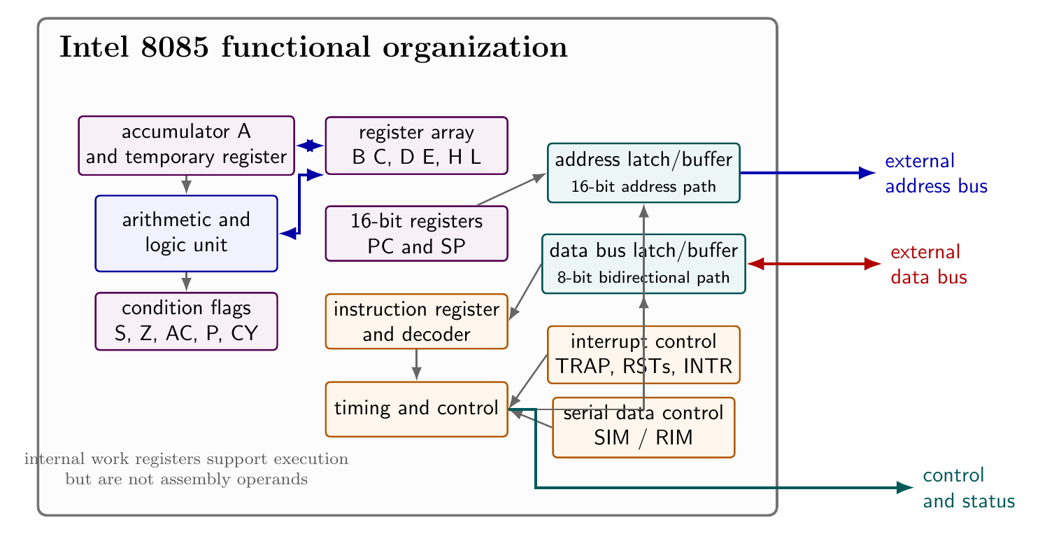
The instruction register and decoder hold and interpret an opcode. The timing and control section then sequences the required register transfers and external cycles. An instruction may need only an internal register operation, or it may require additional memory bytes and bus transactions. Instruction length and execution time are therefore properties of the specific opcode and addressing mode, not merely of the processor’s 8-bit data width.
The ALU performs addition, subtraction, increment, decrement, comparison and bitwise logical operations. The accumulator A is a principal operand and destination for many of these operations. A compare can be regarded as an internal subtraction that updates flags without replacing either programmer-visible operand. Temporary internal registers preserve operands and intermediate values when such an operation would otherwise be destructive.
The address bus latch presents a 16-bit memory address, whereas the data bus latch exchanges one 8-bit quantity with memory or an interface. During an instruction fetch, the processor places the program-counter value on the address path, increments the counter, accepts the returned byte, and decodes it. The word latch emphasizes that an external value must remain defined for the relevant part of the bus transaction even while other internal work proceeds.
The 8085 also incorporates interrupt control, clock/control functions and serial data facilities. Its interrupt priority from highest to lowest is TRAP, RST 7.5, RST 6.5, RST 5.5 and INTR. TRAP is non-maskable; the three restart inputs are separately maskable. The 8085-specific SIM and RIM instructions communicate interrupt-mask/status information and one serial-output or serial-input bit through the accumulator.
Eight-bit registers and sixteen-bit pairs
The accumulator A and six general-purpose registers B, C, D, E, H and L each hold one byte. B–C, D–E and H–L can also be treated as three 16-bit pairs. In a pair, the first named register is the high-order byte and the second is the low-order byte:
\[BC=256B+C,\qquad DE=256D+E,\qquad HL=256H+L.\]Thus, if $B=12_{\mathrm H}$ and $C=34_{\mathrm H}$, then $BC=1234_{\mathrm H}$. A register-pair instruction is not the same as two unrelated 8-bit instructions: INX B, for example, increments the combined BC word, propagating a carry from C into B, and affects none of the condition flags.
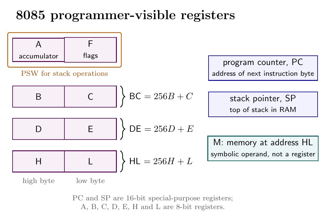
HL has an especially important indirect-address role. When an 8-bit instruction uses the symbolic operand M, the operation applies to the memory byte at address HL. For example, MOV A,M reads the selected memory byte into A, while MOV M,C writes C to that location. M therefore names neither an eighth general-purpose register nor the contents of HL; it denotes an external memory operand selected by the 16-bit value in HL.
The pair symbols depend on the opcode context. ADD B uses the 8-bit B register, but PUSH B places the 16-bit BC pair on the stack. Similarly, H denotes the HL pair in a word operation such as INX H, while M denotes memory through HL in a byte operation. PSW denotes the 16-bit program status word formed by the accumulator and the formatted condition-flag byte for PUSH PSW and POP PSW.
Program counter and stack pointer
PC and SP are 16-bit special-purpose registers. The program counter identifies the next instruction byte. Sequential fetches advance it; jump, call, return, restart and accepted interrupt operations replace it according to their control-flow semantics. PC is therefore not simply “the current instruction address,” because during execution it may already point at a following byte.
The stack pointer addresses the current top of a stack in RAM. The program must initialize SP. A push first moves SP toward lower addresses as two bytes are stored; a pop retrieves two bytes and moves SP toward higher addresses. A call pushes the return address before loading a new PC, and a return pops that saved address into PC. Balanced stack use is essential: if a subroutine pushes a register pair, it must restore the corresponding word before returning.
Intel’s word-storage convention places the least-significant byte at the lower memory address and the most-significant byte at the next higher address. For a word $1234_{\mathrm H}$ stored from address $2500_{\mathrm H}$, memory contains $34_{\mathrm H}$ at $2500_{\mathrm H}$ and $12_{\mathrm H}$ at $2501_{\mathrm H}$. This byte order agrees naturally with L and C being the low bytes of HL and BC.
The five condition flags
The ALU records five one-bit conditions: sign S, zero Z, auxiliary carry AC, parity P and carry CY. They occupy defined positions in the flag byte used by the PSW, with filler positions between them.
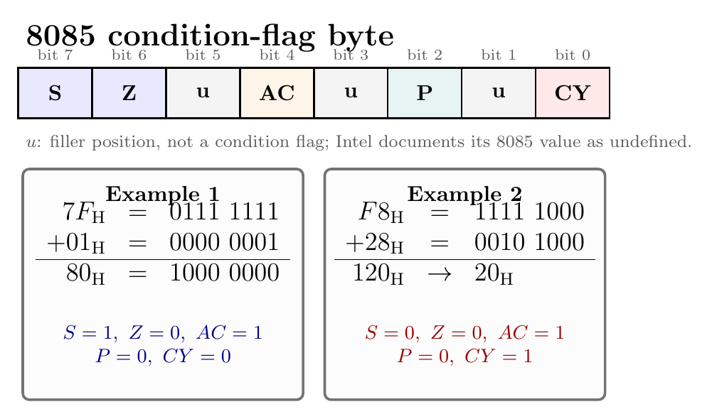
Their meanings are:
- S copies bit 7 of an affected 8-bit result. It supports signed tests when the byte is interpreted in two’s-complement form.
- Z is one exactly when the affected result byte is $00_{\mathrm H}$.
- AC reports a carry out of bit 3 into bit 4. It supports decimal adjustment and cannot be tested directly by a conditional branch.
- P is one for even parity: the result contains an even number of one bits. It is zero for odd parity.
- CY reports a carry out of bit 7 in addition. In subtraction it serves as a borrow indication under the instruction definitions, and rotate instructions can use it as a ninth bit.
The formatted order from bit 7 to bit 0 is
\[\boxed{S\;Z\;u\;AC\;u\;P\;u\;CY},\]where $u$ marks a filler bit rather than a condition flag. Intel documents those filler bits as undefined on the 8085, so a program should not use their saved values as status information.
Flags are meaningful only in relation to the instruction that most recently affected them. Data-transfer operations such as MOV, and input/output transfers, do not generally refresh the arithmetic result flags. INX and DCX preserve all five; DAD affects only CY. Conversely, an 8-bit arithmetic instruction commonly affects Z, S, P, CY and AC. A conditional jump placed after an instruction that preserves flags tests older state, not the transferred data.
Worked flag evaluations
Consider
\[7F_{\mathrm H}+01_{\mathrm H}=80_{\mathrm H}.\]There is no ninth-bit carry, so $CY=0$. The low nibble $F_{\mathrm H}+1$ carries into bit 4, hence $AC=1$. The result is nonzero, so $Z=0$; bit 7 is one, so $S=1$; and $80_{\mathrm H}=1000\,0000_2$ contains one set bit, giving odd parity and $P=0$. The positive signed value $+127$ has overflowed to the two’s-complement pattern for $-128$, but the 8085 has no separate signed-overflow flag. Software must infer signed overflow from operand and result signs.
For a second example,
\[F8_{\mathrm H}+28_{\mathrm H}=120_{\mathrm H}.\]The stored accumulator byte is $20_{\mathrm H}$ and the ninth bit gives $CY=1$. Because $8_{\mathrm H}+8_{\mathrm H}=10_{\mathrm H}$, $AC=1$. The result byte is positive and nonzero, so $S=0$ and $Z=0$. It contains one set bit, so $P=0$. Carry and sign answer different questions: CY concerns unsigned range, whereas S merely reproduces result bit 7.
Register and bus discipline
Efficient assembly programming keeps frequently used bytes in registers, uses register pairs for addresses and counters, and documents which operations destroy A or flags. Register-to-register instructions avoid an external memory access. Memory operands are necessary when the available registers cannot hold the working set, but they add bus activity and require a valid address.
Subroutines should establish a clear preservation convention. A routine that needs BC, DE, HL or PSW can push those resources and pop them in the reverse order before returning. Saving PSW preserves A together with the flags; saving only another register pair does not protect arithmetic status. The stack must reside in writable memory and must not grow into program variables or unmapped space.
Primary sources
- Intel, MCS-80 User’s Manual, October 1977
- Intel, 8080/8085 Assembly Language Programming Manual, November 1978
Preparation questions
- Draw the functional architecture of the 8085 and trace the path followed during an instruction fetch.
- Distinguish programmer-visible registers from the internal temporary registers used by the processor.
- If $D=9A_{\mathrm H}$ and $E=70_{\mathrm H}$, calculate DE and identify its high and low bytes.
- Explain the different meanings of H and M in
INX HandMOV A,M. - Determine S, Z, AC, P and CY after adding $6F_{\mathrm H}$ and $91_{\mathrm H}$ as 8-bit quantities.
- Why can a conditional parity jump immediately after an
INinstruction test stale information? - Explain the roles of PC and SP during a subroutine call and return.
- State the 8085 interrupt priority order and describe the functions exposed by
SIMandRIM.


Discussion