

11 Jun 2025
Inverting and Non-Inverting Operational-Amplifier Circuits
Node-equation derivations with finite open-loop gain, voltage-follower operation, impedances, bandwidth and large-signal limits.
The inverting and non-inverting amplifiers are closed-loop realizations of the same differential relation,
\[v_o=A(v_+-v_-).\]Their ideal formulae follow when the open-loop gain is large, the feedback is negative, and the device remains in its linear operating region. The finite-$A$ derivations below quantify the differential input voltage that is required to generate the output and distinguish signal gain from noise gain.
Inverting amplifier: exact node analysis
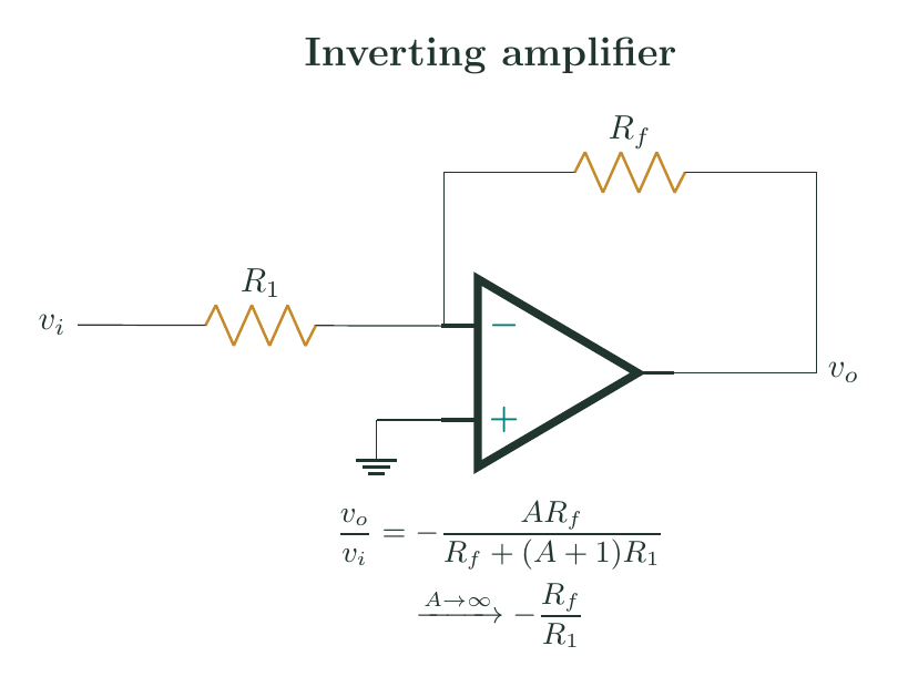
Let $R_1$ connect the source $v_i$ to the inverting node $v_-$, let $R_f$ connect $v_o$ to the same node, and ground the non-inverting input. Assuming zero input current but retaining finite open-loop gain,
\[\frac{v_i-v_-}{R_1}+\frac{v_o-v_-}{R_f}=0, \qquad v_o=-Av_-.\]Substituting $v_-=-v_o/A$ into the node equation gives
\[\frac{v_i+v_o/A}{R_1} +\frac{v_o+v_o/A}{R_f}=0.\]Hence
\[\boxed{ \frac{v_o}{v_i} =-\frac{A R_f}{R_f+(A+1)R_1} }\]or, with $k=R_f/R_1$,
\[\frac{v_o}{v_i}=-\frac{k}{1+(1+k)/A}.\]For $A\gg1+k$,
\[\boxed{\frac{v_o}{v_i}\simeq-\frac{R_f}{R_1}}.\]The inverting node is then close to ground, but is not physically connected to ground. Its exact value is $v_-=-v_o/A$; it is called a virtual ground because its voltage is maintained near zero by feedback while it can neither supply nor absorb current through the op-amp input.
The source current is
\[i_i=\frac{v_i-v_-}{R_1}.\]Using the finite-$A$ solution, the input resistance seen by an ideal voltage source is
\[\boxed{R_{in}\equiv\frac{v_i}{i_i} =R_1+\frac{R_f}{A+1}}.\]It tends to $R_1$, not infinity. The source therefore sees the chosen input resistor even though the op-amp input itself ideally draws no current. If the source has resistance $R_s$, it adds to $R_1$ for gain and noise calculations unless it has already been included in the specified $R_1$.
Current summation and transresistance interpretation
Under the virtual-ground approximation,
\[i_1=\frac{v_i}{R_1},\qquad i_f=\frac{0-v_o}{R_f}.\]Since no current enters the input, $i_1+i_f=0$. Thus the circuit converts an input current to an output voltage:
\[\boxed{v_o=-R_f i_1}.\]This transresistance viewpoint extends naturally to current-output sensors and summing amplifiers. The approximation fails if the required $v_o$ exceeds the output swing or if $i_f$ plus the load current exceeds the output-current capability.
Non-inverting amplifier
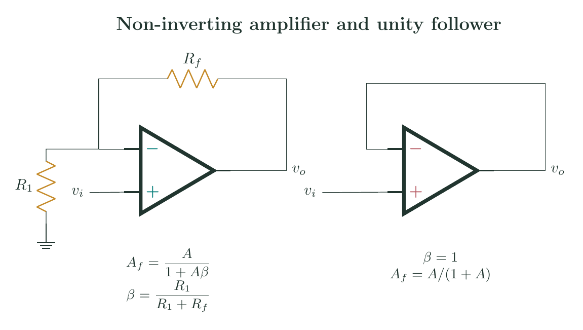
Apply $v_i$ to the non-inverting input. A divider formed by $R_f$ and $R_1$ feeds
\[v_-=\beta v_o,\qquad \beta=\frac{R_1}{R_1+R_f}.\]The open-loop equation is
\[v_o=A(v_i-\beta v_o),\]so
\[\boxed{ \frac{v_o}{v_i}=\frac{A}{1+A\beta} =\frac{1/\beta}{1+1/(A\beta)} }.\]For $A\beta\gg1$,
\[\boxed{\frac{v_o}{v_i}\simeq 1+\frac{R_f}{R_1}}.\]The input resistance is very high because the signal is applied directly to the non-inverting input. If the op amp has finite differential input resistance $R_{id}$, series feedback increases the terminal input resistance approximately to $R_{id}(1+A\beta)$. Practical input resistance is ultimately limited by bias-current paths, protection networks and input capacitance.
Voltage follower
Joining the output directly to the inverting input gives $\beta=1$ and
\[\boxed{A_f=\frac{A}{1+A}}.\]For $A=2\times10^5$, $A_f=0.999995$. The differential error is
\[v_d=v_i-v_o=\frac{v_i}{1+A}.\]The follower buffers a high-resistance source from a low-resistance load. Feedback makes its input resistance high and its closed-loop output resistance approximately $R_o/(1+A)$ at low frequency. A voltage follower does not increase signal voltage, but it can provide current and impedance transformation. It must be specified as unity-gain stable; an uncompensated op amp designed for a minimum noise gain can oscillate in this connection.
Gain error and bandwidth
For an inverting amplifier, setting the independent input source to zero leaves the feedback factor
\[\beta=\frac{R_1}{R_1+R_f}.\]Therefore its noise gain is
\[\boxed{G_N=\frac1\beta=1+\frac{R_f}{R_1}},\]although its signal gain is $-R_f/R_1$. For a one-pole op amp,
\[f_H\simeq\frac{f_t}{G_N}.\]For the non-inverting circuit, signal gain and noise gain are both $1+R_f/R_1$. A compensated capacitance across $R_f$, input capacitance at the summing node, or source impedance changes the frequency dependence of noise gain and requires a full impedance analysis.
As an example, take $R_1=1.00\,\text{k}\Omega$, $R_f=9.00\,\text{k}\Omega$, $A_0=2.00\times10^5$ and $f_t=1.00\,\text{MHz}$. The exact inverting dc gain is
\[A_{v}=-\frac{(2.00\times10^5)(9)}{9+200001} =-8.99955,\]while $G_N=10$ and $f_H\simeq100\,\text{kHz}$. The corresponding non-inverting ideal gain is $10$, with the same noise-gain bandwidth.
Output loading and large-signal restrictions
With a load $R_L$, the ideal gain is unchanged only if the op amp can supply
\[i_o=\frac{v_o}{R_L}+\frac{v_o-v_-}{R_f}.\]The feedback-resistor current is part of the output load and cannot be omitted. Output resistance and current limiting cause additional gain error for heavy loads. The available voltage swing is normally less than the supply rails and depends on load current.
For a sinusoidal output $V_p\sin(2\pi ft)$, linear operation requires
\[2\pi fV_p\leq \mathrm{SR}.\]The full-power bandwidth is consequently
\[\boxed{f_{FP}=\frac{\mathrm{SR}}{2\pi V_p}}.\]It is distinct from small-signal bandwidth. For $V_p=8\,\text{V}$ at $20\,\text{kHz}$, the required slew rate is $1.01\,\text{V}/\mu\text{s}$. An op amp with $0.5\,\text{V}/\mu\text{s}$ will produce a slope-limited waveform even if its small-signal gain-bandwidth product is sufficient.
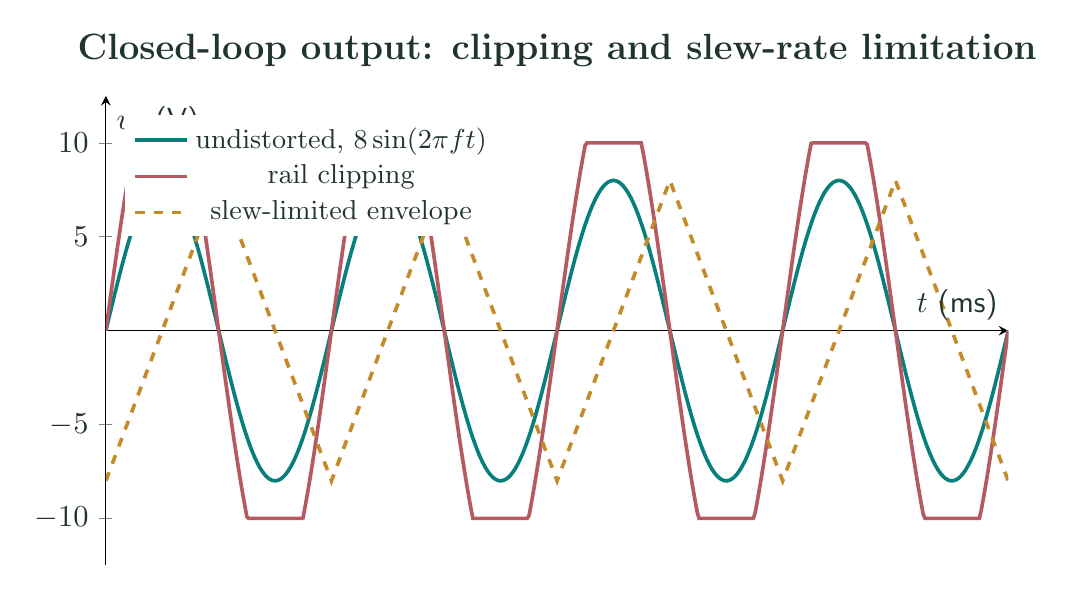
The input common-mode voltage must also remain within the specified range. In a follower it equals the signal voltage, while in an inverting amplifier the summing node stays near the chosen reference. Output phase reversal, input differential protection conduction and recovery from saturation are device-specific effects that cannot be inferred from the ideal op-amp symbol.
Amplification about a nonzero reference
The non-inverting terminal need not be grounded. If it is held at a reference $V_R$, ideal node analysis gives
\[\frac{v_i-V_R}{R_1}+\frac{v_o-V_R}{R_f}=0,\]and hence
\[\boxed{v_o=\left(1+\frac{R_f}{R_1}\right)V_R -\frac{R_f}{R_1}v_i}.\]The circuit inverts and scales the input about $V_R$. It is useful with a single supply, where $V_R$ may be a buffered mid-supply reference. Because any noise or error on $V_R$ is amplified by the noise gain, a high-impedance resistor divider is not automatically an adequate reference. Its Thevenin resistance also interacts with input bias current.
For a non-inverting signal referred to $V_R$, connect the lower feedback resistor to $V_R$ rather than ground. The result can be written
\[\boxed{v_o-V_R=\left(1+\frac{R_f}{R_1}\right)(v_i-V_R)}.\]This form makes the operating-point translation explicit and helps test whether input common-mode and output-swing limits are satisfied.
Resistor tolerance and gain uncertainty
For the ideal inverting magnitude $k=R_f/R_1$, small independent resistance changes give
\[\frac{\Delta k}{k}\simeq \frac{\Delta R_f}{R_f}-\frac{\Delta R_1}{R_1}.\]If each resistor has tolerance $t$, the worst-case ratio error is approximately $2t$; an uncorrelated root-sum-square estimate is $\sqrt{2}t$. Matched networks can have modest absolute tolerance but excellent ratio tolerance and temperature tracking. The finite-open-loop-gain error must be added to the ratio error with its own sign or bounded separately.
The resistor values also determine noise and loading. Scaling both $R_1$ and $R_f$ upward preserves ideal gain but raises Johnson voltage noise and makes bias-current error larger. Scaling them downward increases feedback current, output loading and source loading. Practical values are selected from all of these constraints, not from the gain ratio alone.
Parasitic capacitance makes the ratio frequency dependent. A capacitance $C_f$ across $R_f$ changes the feedback impedance to $R_f/(1+sR_fC_f)$ and deliberately reduces high-frequency signal gain. Capacitance at the inverting node instead modifies noise gain and may create a rising high-frequency section. The two capacitances therefore cannot be treated as interchangeable even when their nominal corner frequencies are similar.
Closed-loop output resistance
Let the op amp have small-signal open-loop output resistance $r_o$. Applying a test current at the output with the signal source set to zero changes the differential input by $-\beta v_o$. The controlled source opposes the test-induced output change, and the closed-loop resistance is approximately
\[\boxed{r_{of}=\frac{r_o}{1+A\beta}}.\]This result applies inside the loop bandwidth. At high frequency $\lvert A\beta\rvert$ falls, so output impedance rises and may become inductive because of loop phase. The dc expression therefore cannot be used to predict the interaction with a capacitive load without the full complex loop gain.
Preparation questions
- Obtain the exact inverting gain for finite $A$ directly from KCL, and identify its fractional error from $-R_f/R_1$.
- Derive the finite-$A$ input resistance of the inverting amplifier.
- An amplifier has $R_1=2\,\text{k}\Omega$, $R_f=38\,\text{k}\Omega$, $A_0=10^5$ and $f_t=4\,\text{MHz}$. Calculate dc signal gain, noise gain and one-pole bandwidth.
- Explain why the voltage follower can deliver power gain although its voltage gain is nearly unity.
- Include the feedback current when finding the peak output current for a loaded non-inverting amplifier.
- Find the full-power bandwidth for a $10\,\text{V}$ peak output when $\mathrm{SR}=2\,\text{V}/\mu\text{s}$.


Discussion