

13 Jun 2025
Operational-Amplifier Input Offset and Bias Currents
Input offset voltage, bias and offset currents, compensation resistance, total output offset, drift and error budgeting.
A practical operational amplifier gives a nonzero dc output even when the intended differential input is zero. Transistor mismatch produces an input offset voltage, and the input devices require bias currents. Negative feedback amplifies these small input errors according to the circuit’s noise gain. Their signs are not normally known in advance, so typical calculations predict a nominal value only when measured signs are supplied; guaranteed design uses worst-case magnitudes.
Input offset voltage
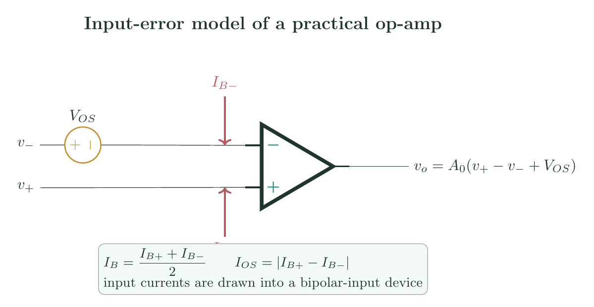
The input offset voltage $V_{OS}$ is the differential dc voltage that must be applied between the inputs to force the output to zero under specified conditions. A convenient model places a small voltage source in series with one input:
\[v_o=A(v_+-v_-+V_{OS}).\]The sign of $V_{OS}$ in this equation is a convention. Datasheets usually specify $\lvert V_{OS}\rvert$ rather than its polarity. In a closed-loop amplifier, the output contribution is approximately
\[\boxed{v_{o,OS}=G_N V_{OS}},\]where $G_N=1/\beta$ is the noise gain. Thus an inverting signal gain $-R_f/R_1$ has offset-voltage gain $1+R_f/R_1$, not $R_f/R_1$.
Input bias and input offset currents
Let $I_{B+}$ and $I_{B-}$ be the dc currents at the non-inverting and inverting terminals. For a bipolar-input op amp they conventionally flow into the device. The input bias current is their average magnitude,
\[\boxed{I_B=\frac{I_{B+}+I_{B-}}{2}},\]and the input offset current is their mismatch,
\[\boxed{I_{OS}=\lvert I_{B+}-I_{B-}\rvert}.\]$I_{OS}$ is not an additional physical current entering a third terminal. It measures the imperfect tracking of the two bias currents. FET- and CMOS-input amplifiers can have much smaller room-temperature bias current, but leakage often rises strongly with temperature. Bias-current sign can also differ among input architectures, so the datasheet convention must be checked.
When an input current flows through the Thevenin resistance connected to its terminal, it creates an input voltage error. Therefore high source resistance makes bias-current error important even if the current is only nanoamperes or picoamperes.
Complete inverting-amplifier offset equation
Consider an inverting amplifier with the intended input grounded through $R_1$, feedback resistance $R_f$, and a compensating resistance $R_B$ from the non-inverting terminal to ground. Let input currents flow into the op amp. KCL at the non-inverting node gives
\[v_+=-I_{B+}R_B.\]At the inverting node,
\[\frac{v_-}{R_1}+\frac{v_--v_o}{R_f}+I_{B-}=0.\]For large loop gain, the error model imposes
\[v_-=v_++V_{OS}=V_{OS}-I_{B+}R_B.\]Solving the node equation gives the total dc output offset
\[\boxed{ v_{o,\mathrm{off}}=\left(1+\frac{R_f}{R_1}\right) (V_{OS}-I_{B+}R_B)+I_{B-}R_f }.\]Equivalently,
\[v_{o,\mathrm{off}}=G_N V_{OS} -G_N I_{B+}R_B+I_{B-}R_f.\]For a finite constant open-loop gain, every right-hand contribution is multiplied by the factor
\[\frac{A\beta}{1+A\beta};\]the infinite-$A$ result is normally adequate because the dc loop gain is large.
Bias-current compensation
Choose the resistance at the non-inverting terminal equal to the resistance seen at the inverting terminal when independent sources are set to zero:
\[\boxed{R_B=R_1\parallel R_f =\frac{R_1R_f}{R_1+R_f}}.\]Since
\[G_N(R_1\parallel R_f)=R_f,\]the current terms become
\[-I_{B+}R_f+I_{B-}R_f =(I_{B-}-I_{B+})R_f.\]Thus
\[\boxed{v_{o,\mathrm{off}}=G_NV_{OS} +(I_{B-}-I_{B+})R_f}.\]The contribution of the average bias current cancels; the residual is governed by input offset current. Compensation does not cancel $V_{OS}$ and is ineffective if the two bias currents do not track.
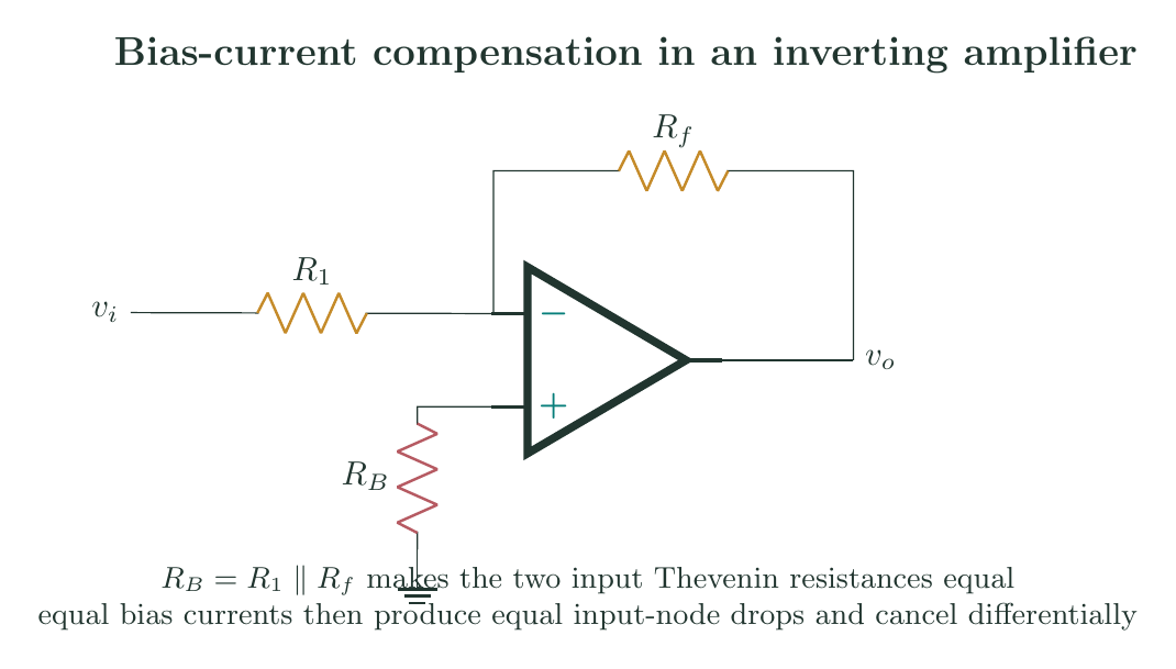
If the source has Thevenin resistance $R_s$, the resistance on the inverting side is $(R_s+R_1)\parallel R_f$, and $R_B$ should match that value. In ac-coupled circuits, the relevant dc resistance may differ from the midband signal impedance because capacitors open at dc. A resistance inserted for compensation contributes Johnson noise; with very small bias-current op amps it may worsen total accuracy rather than improve it.
Worked offset calculation
Let
\[R_1=10.0\,\text{k}\Omega,\quad R_f=100\,\text{k}\Omega, \quad V_{OS}=0.50\,\text{mV},\] \[I_{B+}=80\,\text{nA},\qquad I_{B-}=86\,\text{nA}.\]The noise gain is $G_N=11$. Without $R_B$,
\[v_{o,\mathrm{off}}=(11)(0.50\,\text{mV}) +(86\,\text{nA})(100\,\text{k}\Omega) =14.10\,\text{mV}.\]With
\[R_B=10\,\text{k}\Omega\parallel100\,\text{k}\Omega =9.091\,\text{k}\Omega,\]the current contribution is
\[(86-80)\,\text{nA}\times100\,\text{k}\Omega =0.60\,\text{mV}.\]Therefore
\[\boxed{v_{o,\mathrm{off}}=5.50\,\text{mV}+0.60\,\text{mV} =6.10\,\text{mV}}.\]The numerical signs assume the polarity convention used in the model. If only maximum magnitudes are specified, a safe bound after compensation is
\[\boxed{\lvert v_{o,\mathrm{off}}\rvert \leq G_N\lvert V_{OS}\rvert_{\max}+R_f I_{OS,\max}}.\]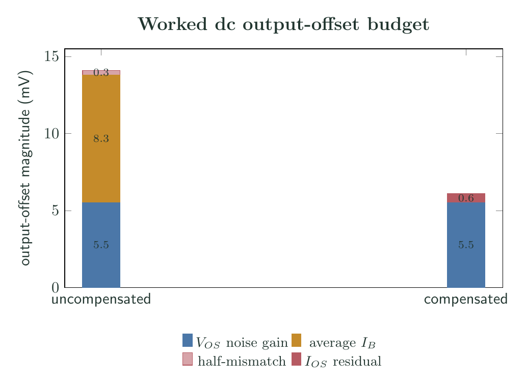
Temperature drift and source-resistance error
Offset voltage depends on temperature. If the local model is
\[V_{OS}(T)=V_{OS}(T_0)+\alpha_{OS}(T-T_0),\]then the output drift contribution is $G_N\alpha_{OS}\Delta T$. Bias currents and $I_{OS}$ also drift, generally nonlinearly. Guaranteed precision over a temperature interval must use the datasheet limits over that interval rather than extrapolating a room-temperature typical value.
Input offset can also arise from source-resistance imbalance even if $I_{B+}=I_{B-}$. If the dc Thevenin resistances are $R_{T+}$ and $R_{T-}$, equal bias currents produce an approximate differential error
\[v_{d,B}=I_B(R_{T-}-R_{T+}).\]The corresponding output term is $G_Nv_{d,B}$. Thermoelectric junction voltages, leakage over contaminated circuit boards and resistor self-heating may exceed the intrinsic op-amp offset in microvolt-level designs.
Input offset should also be distinguished from output zero error caused by finite power-supply rejection. Supply changes generate an additional input-referred term, customarily obtained from the specified PSRR, while common-mode changes produce an error through finite CMRR. A complete dc budget refers every error to the input, combines known correlated signs algebraically, bounds unknown signs conservatively, and then applies noise gain.
Exact finite-gain correction
The finite-$A$ result can be obtained without setting the two input voltages equal. From the inverting-node equation,
\[v_o=G_Nv_-+R_fI_{B-},\]while
\[v_-=v_++V_{OS}-\frac{v_o}{A}, \qquad v_+=-I_{B+}R_B.\]Substitution gives
\[v_o\left(1+\frac{G_N}{A}\right) =G_N(V_{OS}-I_{B+}R_B)+R_fI_{B-}.\]Therefore
\[\boxed{ v_{o,\mathrm{off}}= \frac{A}{A+G_N} \left[G_N(V_{OS}-I_{B+}R_B)+R_fI_{B-}\right] }.\]The factor $A/(A+G_N)$ approaches unity at dc. This derivation also shows that the appropriate comparison is $A/G_N$, the loop gain, not $A$ alone.
Worst-case and statistical error budgets
If the polarities of $V_{OS}$ and $I_{OS}$ are unknown, a guaranteed compensated bound is the sum of magnitudes,
\[E_{o,\max}=G_N V_{OS,\max}+R_f I_{OS,\max}.\]For independent, zero-mean random production spreads with known standard deviations, a statistical estimate may instead use
\[\sigma_o=\sqrt{(G_N\sigma_{VOS})^2 +(R_f\sigma_{IOS})^2}.\]This root-sum-square expression is not a substitute for datasheet maximum limits. It is appropriate only when the distributions and independence assumptions are justified. Systematic thermocouple or leakage errors must be added with their actual signs.
Offset trimming and stabilized amplifiers
Some op amps expose offset-null terminals that permit a small internal balance adjustment. The manufacturer-specified network must be used because arbitrary external current can disturb the input stage. Trimming at one temperature cancels the initial offset but not necessarily temperature drift.
Auto-zero amplifiers periodically sample and correct their offset; chopper-stabilized amplifiers modulate low-frequency input signals away from the region dominated by offset and $1/f$ noise. These techniques greatly reduce low-frequency error but can introduce switching ripple, charge-injection current and spectral artifacts. A precision design must compare offset, drift, bias current, voltage noise, current noise and source resistance over the actual signal bandwidth.
Bias-current transients with input capacitance
Bias current is a dc specification, but it can also charge an input coupling or sensor capacitance. If a current step $\Delta I_B$ flows into an otherwise isolated capacitance $C_s$, the input error initially changes at
\[\frac{dv_e}{dt}=\frac{\Delta I_B}{C_s}.\]A resistance $R_s$ in parallel eventually limits the change to approximately $\Delta I_B R_s$ with time constant $R_sC_s$. This mechanism matters in sample-and-hold circuits, photodiode amplifiers and sensors that become high impedance after a switch opens. Input-current pulses specified for chopper devices can create larger dynamic errors than their average bias current suggests.
Offset correction at the output is safe only when referred back through the correct noise gain. A measured $20\,\text{mV}$ output offset at noise gain $100$ represents $200\,\mu\text{V}$ input-referred offset, but the same output reading at noise gain $2$ represents $10\,\text{mV}$. Reporting only output offset without circuit gain obscures the quality of the amplifier and prevents comparison between configurations.
Preparation questions
- Starting from the two node equations, derive the total output offset of an inverting amplifier with $R_B$.
- Prove that $G_N(R_1\parallel R_f)=R_f$.
- For $R_1=5\,\text{k}\Omega$, $R_f=200\,\text{k}\Omega$, $V_{OS}=200\,\mu\text{V}$, $I_B=20\,\text{nA}$ and $I_{OS}=3\,\text{nA}$, find uncompensated and compensated bounds.
- Explain why input offset current cannot be added independently to both input bias currents.
- Include a source resistance $R_s$ and obtain the correct compensation resistor.
- An op amp has offset drift $2\,\mu\text{V}/^\circ\text{C}$ and noise gain $50$. Find the output change over $40^\circ\text{C}$, ignoring current drift.


Discussion