

17 Jun 2025
Operational-Amplifier Integrators and Differentiators
Ideal and band-limited active integration and differentiation, transfer functions, initial conditions, frequency response, waveform conversion and non-ideal design limits.
An operational amplifier with frequency-dependent input or feedback impedance can realize temporal integration and differentiation over a prescribed frequency band. The ideal circuits express the mathematical operations exactly within the ideal op-amp model; practical circuits introduce resistors and capacitors that bound the gain, suppress drift and noise, and improve stability.
General inverting impedance relation
For an ideal inverting configuration with input impedance $Z_i(s)$ and feedback impedance $Z_f(s)$, the summing node is at virtual ground and draws no current. KCL gives
\[\frac{v_i}{Z_i}+\frac{v_o}{Z_f}=0,\]so
\[\boxed{H(s)\equiv\frac{V_o(s)}{V_i(s)} =-\frac{Z_f(s)}{Z_i(s)}}.\]This relation is valid only where loop gain is large enough to maintain the summing node and where the output remains linear. The initial charge of a feedback capacitor must be included separately when solving a time-domain initial-value problem.
Ideal operational-amplifier integrator
Use an input resistor $R$ and a feedback capacitor $C$. Then
\[Z_i=R,\qquad Z_f=\frac{1}{sC},\]and
\[\boxed{H_I(s)=-\frac{1}{sRC}}.\]In the time domain, KCL at the summing node gives
\[\frac{v_i(t)}{R}=-C\frac{dv_o}{dt},\]whence
\[\boxed{ v_o(t)=v_o(t_0)-\frac{1}{RC} \int_{t_0}^{t}v_i(t')\,dt' }.\]The constant $v_o(t_0)$ is set by the initial capacitor voltage. For a constant input $V$, the output is a ramp of slope $-V/(RC)$. A symmetrical square wave produces a triangular output because the ramp slope reverses whenever the input changes sign.
For $s=j\omega$,
\[H_I(j\omega)=\frac{j}{\omega RC},\]so
\[\lvert H_I\rvert=\frac{1}{\omega RC},\qquad \angle H_I=+90^\circ.\]The plus-$90^\circ$ phase follows from the inverting sign combined with the capacitor’s $-90^\circ$ factor. Magnitude falls at $20\,\text{dB/decade}$.
Why the ideal integrator is not a dc amplifier
At $s=0$, the feedback capacitor is open and the ideal circuit has infinite noise gain. Any input offset voltage or bias-current imbalance charges the capacitor continuously, causing the output to drift to a supply rail. The ideal model also provides no dc path to establish the input operating point. A large resistor $R_f$ placed in parallel with $C$ supplies dc feedback.
For the practical integrator,
\[Z_f=R_f\parallel\frac1{sC} =\frac{R_f}{1+sR_fC}.\]With input resistor $R$,
\[\boxed{ H_{PI}(s)=-\frac{R_f/R}{1+sR_fC} }.\]At low frequency,
\[H_{PI}\simeq-\frac{R_f}{R},\]so dc gain is finite. For
\[\omega\gg\omega_L=\frac{1}{R_fC},\]the transfer becomes
\[H_{PI}\simeq-\frac{1}{sRC},\]and integration is obtained. The useful upper frequency is limited by op-amp loop gain, slew rate and parasitic capacitance rather than by this first-order feedback network alone.
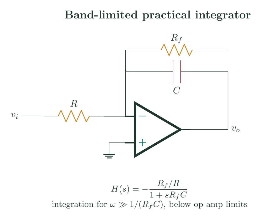
For example, choose $R=10\,\text{k}\Omega$, $C=10\,\text{nF}$ and $R_f=1.0\,\text{M}\Omega$. Then
\[f_L=\frac{1}{2\pi R_fC}=15.9\,\text{Hz}.\]At $1.00\,\text{kHz}$, $\omega R_fC=62.8$, so the circuit closely approximates an integrator. For a $1.00\,\text{V}$ square-wave level lasting half a period at $1.00\,\text{kHz}$,
\[\Delta v_o=-\frac{V}{RC}\frac{1}{2f} =-5.00\,\text{V}.\]The predicted $5.00\,\text{V}$ peak-to-peak triangle must fit inside the available output swing.
Ideal operational-amplifier differentiator
Use an input capacitor $C$ and feedback resistor $R_f$. Then
\[Z_i=\frac1{sC},\qquad Z_f=R_f,\]so
\[\boxed{H_D(s)=-sR_fC}.\]In the time domain,
\[\boxed{v_o(t)=-R_fC\frac{dv_i}{dt}}.\]For a ramp $v_i=mt+b$, the output is the constant $-R_fCm$. A triangular input produces an approximately square output. An ideal step has a delta-function derivative; a physical circuit instead produces a finite pulse governed by rise time and bandwidth.
For sinusoidal excitation,
\[H_D(j\omega)=-j\omega R_fC,\]so magnitude rises at $20\,\text{dB/decade}$ and phase is $-90^\circ$. This increasing high-frequency gain amplifies noise and parasitic pickup. Moreover, the noise gain rises with frequency because the input capacitance becomes a small impedance, degrading phase margin.
Band-limited practical differentiator
Place a resistor $R_1$ in series with the input capacitor $C_1$, and place a capacitor $C_f$ in parallel with $R_f$. The impedances are
\[Z_i=R_1+\frac1{sC_1} =\frac{1+sR_1C_1}{sC_1},\] \[Z_f=R_f\parallel\frac1{sC_f} =\frac{R_f}{1+sR_fC_f}.\]Therefore
\[\boxed{ H_{PD}(s)= -\frac{sR_fC_1} {(1+sR_1C_1)(1+sR_fC_f)} }.\]When
\[\omega\ll\min\left\{\frac1{R_1C_1}, \frac1{R_fC_f}\right\},\]both denominator factors are nearly unity and $H_{PD}\simeq-sR_fC_1$. At high frequency the input resistor prevents $Z_i$ from vanishing, while $C_f$ reduces feedback impedance. The two poles restrict high-frequency gain and improve noise and stability behavior.
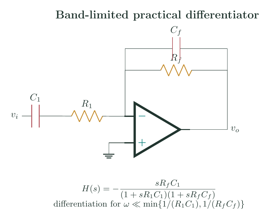
Take $R_1=10\,\text{k}\Omega$, $C_1=10\,\text{nF}$, $R_f=100\,\text{k}\Omega$, and $C_f=100\,\text{pF}$. The pole frequencies are
\[f_1=\frac1{2\pi R_1C_1}=1.59\,\text{kHz},\] \[f_2=\frac1{2\pi R_fC_f}=15.9\,\text{kHz}.\]Accurate differentiation requires frequencies appreciably below $1.59\,\text{kHz}$. At frequencies between the poles, the first denominator factor changes the rising response toward a plateau; above the second pole the response rolls off.
Waveform relations and scaling
For an ideal integrator driven by a symmetrical square wave of amplitude $V_p$ and frequency $f$, the output changes by
\[\lvert\Delta v_o\rvert=\frac{V_p}{2fRC}\]during each half-period. This is the triangle’s peak-to-peak excursion when consecutive ramps join without a dc offset. Thus
\[\boxed{V_{o,pp}=\frac{V_p}{2fRC}}.\]For a triangular input of peak value $V_p$ and frequency $f$, the magnitude of each slope is $4fV_p$. An ideal differentiator gives square-wave magnitude
\[\boxed{\lvert V_o\rvert=4fR_fCV_p}.\]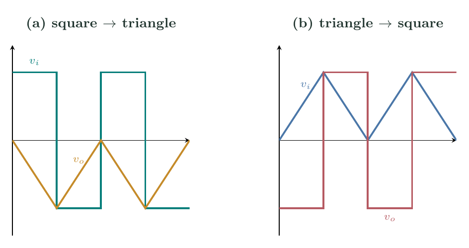
Non-ideal error mechanisms
Input offset and bias-current mismatch generate a nearly constant error current in an integrator. In the ideal circuit this produces a ramp; in the practical circuit $R_f$ limits the final offset. Capacitor leakage and dielectric absorption alter long-time integration, and the initial capacitor voltage fixes the integration constant. The capacitor voltage rating and polarity must be respected.
In a differentiator, broadband input voltage noise is weighted increasingly at high frequency within the differentiation band. Resistor thermal noise, op-amp voltage-noise density and input-current noise must be propagated through their own noise gains. The finite gain-bandwidth product creates additional magnitude and phase error, while capacitive summing-node loading can reduce phase margin. Output slew rate must exceed the demanded waveform slope, and pulse outputs from fast edges must stay within voltage and current limits.
The frequency domain and time domain must remain consistent. Multiplication by $s$ corresponds to differentiation only when initial-condition impulses are treated properly; division by $s$ corresponds to integration with an integration constant. A practical network realizes these operations over a finite band, not for arbitrary signals of infinite bandwidth.
Quantitative approximation errors
Let $x=\omega R_fC$ for the practical integrator. Relative to the ideal integrator magnitude $1/(\omega RC)$,
\[\frac{\lvert H_{PI}\rvert}{1/(\omega RC)} =\frac{x}{\sqrt{1+x^2}}.\]For $x\gg1$, the fractional magnitude shortfall is approximately $1/(2x^2)$, and the phase differs from $+90^\circ$ by approximately $1/x$ radians. Requiring less than $1\%$ magnitude error gives $x\gtrsim7.02$. Thus merely operating at the corner frequency is not sufficient for accurate integration.
For the practical differentiator, define $x_1=\omega R_1C_1$ and $x_2=\omega R_fC_f$. Relative to the ideal differentiator magnitude $\omega R_fC_1$,
\[\boxed{ \frac{\lvert H_{PD}\rvert}{\omega R_fC_1} =\frac{1}{\sqrt{(1+x_1^2)(1+x_2^2)}} }.\]Both $x_1$ and $x_2$ must be small for accurate differentiation. This formula permits an error band to be specified quantitatively instead of identifying the pole frequencies alone.
Finite-open-loop-gain correction
Retaining zero input current but using $v_o=-Av_-$ in the general inverting impedance circuit gives
\[\frac{v_i-v_-}{Z_i}+\frac{v_o-v_-}{Z_f}=0.\]Solving exactly,
\[\boxed{ \frac{v_o}{v_i}=-\frac{Z_f}{Z_i} \frac{A}{A+1+Z_f/Z_i} }.\]The ideal transfer is multiplied by $A/(A+G_N)$, where
\[G_N(s)=1+\frac{Z_f(s)}{Z_i(s)}.\]Because $A(s)$ and $G_N(s)$ are complex and frequency dependent, this factor creates both amplitude and phase error. It also shows why stability analysis of an integrator or differentiator must use the impedance-dependent noise gain rather than the desired mathematical signal transfer alone.
For design, the mathematical-operation band should lie comfortably inside the network asymptotes and the op amp’s loop bandwidth. A decade separation from a first-order corner gives $x=10$: the practical integrator has about $0.50\%$ magnitude error from its dc-limiting pole, while a practical differentiator with both pole ratios below $0.1$ has about $1\%$ combined magnitude shortfall. Additional finite-$A$ error must still be evaluated from the last boxed expression.
Preparation questions
- Derive the ideal integrator transfer function by KCL and retain the initial capacitor voltage in the time-domain result.
- Obtain the practical-integrator transfer function and identify its low- and high-frequency asymptotes.
- A $2\,\text{V}$ peak, $500\,\text{Hz}$ square wave drives an integrator with $R=20\,\text{k}\Omega$ and $C=50\,\text{nF}$. Find the triangular output excursion per half-cycle.
- Derive the two-pole practical-differentiator transfer function from its impedances.
- Determine the square-wave output amplitude when a $1\,\text{V}$ peak, $2\,\text{kHz}$ triangle drives an ideal differentiator with $R_fC=20\,\mu\text{s}$.
- Explain separately how $R_f$ in a practical integrator and $R_1,C_f$ in a practical differentiator improve real-circuit behavior.


Discussion