

09 Jun 2025
Operational Amplifier Negative Feedback, Finite Gain and Stability
Exact feedback equations, loop gain, desensitivity, noise gain, gain-bandwidth relation and elementary stability criteria for voltage-feedback operational amplifiers.
An operational amplifier is fundamentally a very-high-gain differential voltage amplifier. Its open-loop equation in the linear region is
\[v_o(s)=A(s)\,[v_+(s)-v_-(s)],\]where $A(s)$ is the frequency-dependent open-loop gain. The familiar statements $v_+=v_-$ and $i_+=i_-=0$ are not independent laws. Zero input current is an ideal input-resistance approximation, while $v_+\simeq v_-$ is a consequence of large loop gain under stable negative feedback. Beginning with the exact feedback equations prevents these approximations from being applied to a saturated or unstable circuit.
Feedback equation and closed-loop gain
For voltage-series feedback, a fraction $\beta(s)v_o$ of the output is returned to the inverting input. With $v_e=v_s-\beta v_o$,
\[v_o=A(v_s-\beta v_o).\]Therefore
\[\boxed{A_f(s)\equiv\frac{v_o}{v_s} =\frac{A(s)}{1+A(s)\beta(s)}}.\]The dimensionless quantity
\[\boxed{T(s)=A(s)\beta(s)}\]is the loop gain. The return difference is $1+T$. If $\lvert T\rvert\gg1$ at the signal frequency,
\[A_f=\frac{1}{\beta}\frac{T}{1+T} =\frac{1}{\beta}\left(1-\frac{1}{T}+O(T^{-2})\right).\]Thus the feedback network, rather than the poorly controlled open-loop gain, fixes the leading closed-loop gain. The exact fractional shortfall from $1/\beta$ is
\[\boxed{\frac{\beta^{-1}-A_f}{\beta^{-1}}=\frac{1}{1+T}}.\]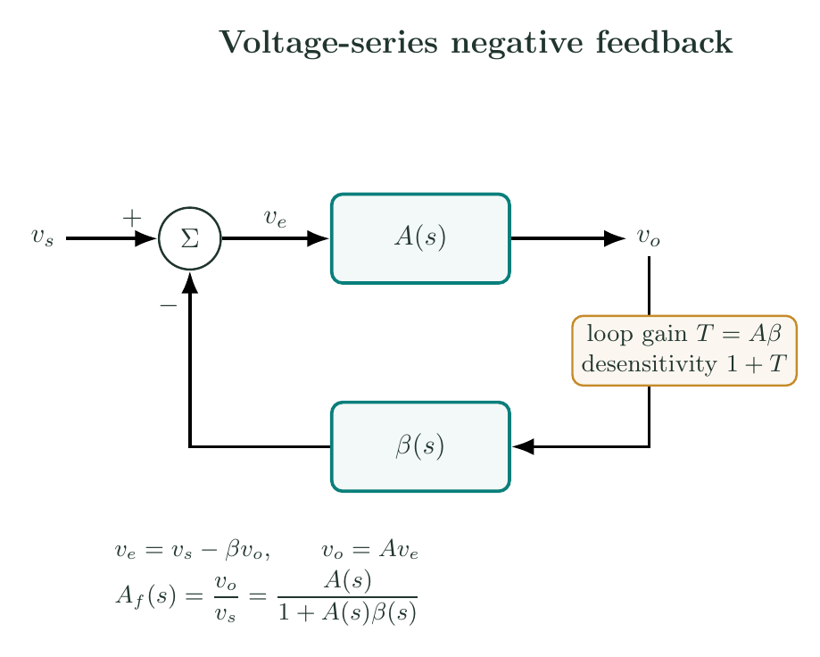
Desensitivity and disturbance rejection
Differentiate $A_f=A/(1+A\beta)$ while holding $\beta$ fixed:
\[\frac{dA_f}{A_f}=\frac{1}{1+A\beta}\frac{dA}{A}.\]The sensitivity of closed-loop gain to open-loop gain is therefore
\[\boxed{S_A^{A_f}\equiv \frac{dA_f/A_f}{dA/A}=\frac{1}{1+T}}.\]A $10\%$ change of $A$ causes only about $0.01\%$ change of $A_f$ when $T=999$. A disturbance $v_n$ inserted at the amplifier input is amplified by $A/(1+T)$, whereas a disturbance added directly in series with the output appears with the factor $1/(1+T)$. Feedback does not remove noise already contained in the source; its location in the loop matters.
For a voltage amplifier, voltage-series feedback raises the input resistance and lowers the output resistance approximately as
\[R_{if}=R_i(1+T),\qquad R_{of}=\frac{R_o}{1+T},\]provided the loop-gain description is evaluated with the correct loading and the feedback topology remains voltage sampling with series mixing.
Closed-loop gain with a dominant pole
A compensated voltage-feedback op amp is often represented over its useful range by
\[A(s)=\frac{A_0}{1+s/\omega_p},\]where $A_0$ is the dc gain and $\omega_p$ the dominant pole. Substitution gives
\[A_f(s)=\frac{A_0}{1+A_0\beta} \frac{1}{1+s/[\omega_p(1+A_0\beta)]}.\]Consequently,
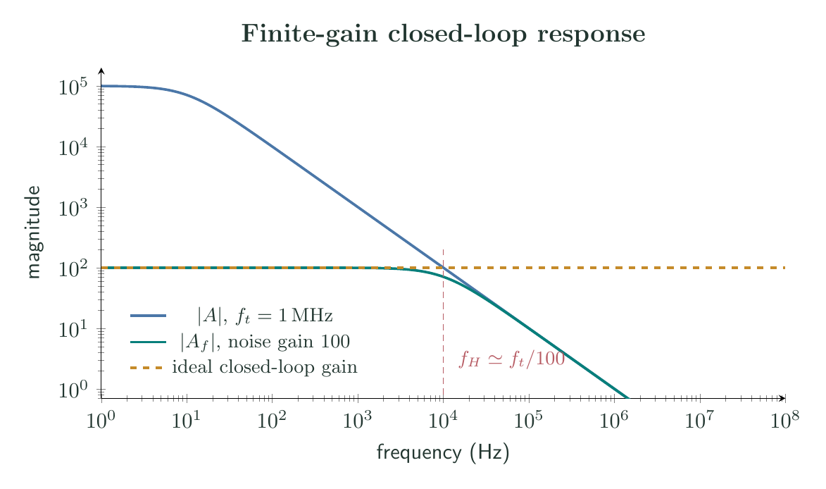
\[A_f(0)=\frac{A_0}{1+A_0\beta},\qquad \omega_H=\omega_p(1+A_0\beta).\]The unity-gain angular frequency is approximately $\omega_t=A_0\omega_p$. When $A_0\beta\gg1$,
\[\boxed{\lvert A_f(0)\rvert\,f_H\simeq f_t}.\]This gain-bandwidth product is a consequence of the one-pole approximation. It is not exact near additional poles and zeros, and it applies to the noise gain rather than necessarily the signal gain.
Signal gain and noise gain
The noise gain is the closed-loop gain from a small voltage inserted in series with an op-amp input to the output. It is also $1/\beta$ when independent signal sources are set to zero. For a non-inverting amplifier it equals the signal gain,
\[G_N=1+\frac{R_f}{R_1}.\]For an inverting amplifier the signal gain is $-R_f/R_1$, but the noise gain remains
\[\boxed{G_N=1+\frac{R_f}{R_1}}.\]Thus an inverting gain of $-0.1$ still has noise gain $1.1$, not $0.1$. Bandwidth, input-referred offset amplification and stability are governed by $G_N$. Reactive source or feedback impedances make $G_N(s)$ frequency dependent, so stability must be assessed from $T=A/G_N$ rather than from the low-frequency signal gain alone.
Loop stability
Negative feedback at low frequency can become positive feedback if accumulated phase lag approaches $180^\circ$. With the return signal subtracted, the characteristic equation is
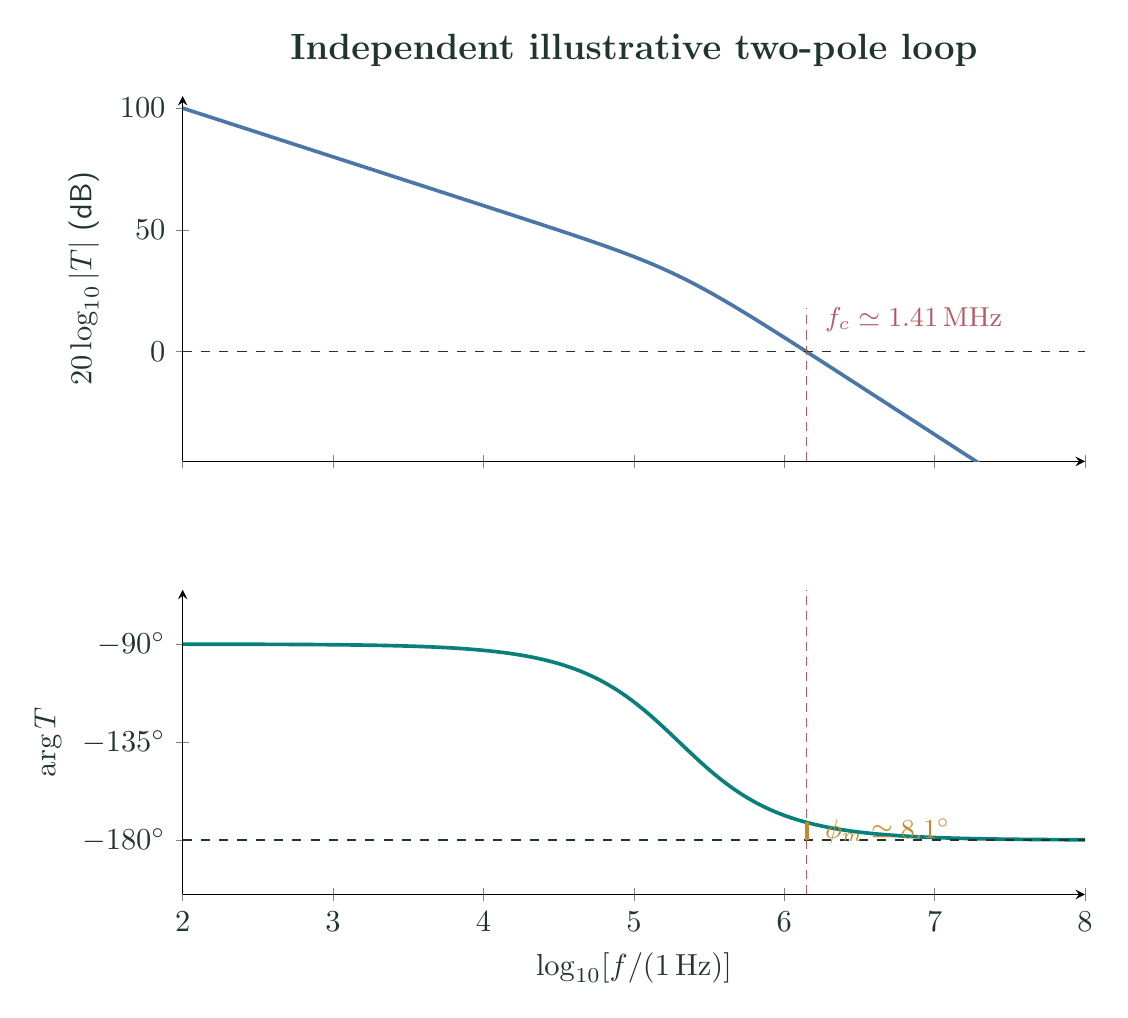
\[\boxed{1+T(s)=0}.\]The circuit is stable only when all roots of this equation lie in the left half of the complex $s$-plane. In frequency-domain design, let $\omega_c$ satisfy $\lvert T(j\omega_c)\rvert=1$. The phase margin is
\[\boxed{\phi_m=180^\circ+\arg T(j\omega_c)}.\]At the phase-crossover frequency $\omega_{180}$ where $\arg T=-180^\circ$, the gain margin is
\[\boxed{G_m=-20\log_{10}\lvert T(j\omega_{180})\rvert\ \text{dB}}.\]Positive margins are necessary practical measures, although a complete test for complicated loops is the Nyquist criterion or a root calculation. Roughly $45^\circ$ to $60^\circ$ phase margin is commonly chosen to limit ringing and overshoot. A second pole close to crossover steepens the loop-magnitude slope toward $-40\,\text{dB/decade}$ and adds phase lag; capacitive loads, device output resistance and feedback capacitance can all introduce such poles.
Numerical design example
Consider $A_0=2.0\times10^5$, $f_t=1.0\,\text{MHz}$ and a resistive feedback network with $G_N=100$, so $\beta=0.01$. The dc loop gain is $T_0=2000$ and
\[A_f(0)=\frac{2.0\times10^5}{1+2000}=99.9500.\]The gain error relative to $100$ is $4.998\times10^{-4}$, or approximately $0.050\%$. Since $f_p=f_t/A_0=5\,\text{Hz}$,
\[f_H=f_p(1+T_0)=10.005\,\text{kHz},\]consistent with $f_t/G_N$. If an additional pole is at $200\,\text{kHz}$, the phase contribution of that pole at crossover is $-\tan^{-1}(f_c/200\,\text{kHz})$. The actual crossover and phase margin must then be found from the full loop-gain magnitude; the simple gain-bandwidth estimate alone does not establish stability.
Conditions for valid linear feedback
The exact small-signal equations presume that the output remains inside its voltage swing, the output current remains below its limit, the input common-mode voltage lies within its specified range, and the differential input does not activate protection structures. For a sinusoidal output $v_o=V_p\sin(2\pi ft)$, the required maximum slope is
\[\boxed{\left\lvert\frac{dv_o}{dt}\right\rvert_{\max}=2\pi fV_p}.\]It must be smaller than the slew rate. Slew-rate distortion is a nonlinear large-signal effect and is not predicted by the small-signal Bode plot. Similarly, saturation opens the effective feedback relation because further input-error changes no longer produce the linear output $A(v_+-v_-)$.
Return-ratio evaluation in a real circuit
The symbol $A\beta$ is exact only when $A$ and $\beta$ are defined with the loading they impose on one another. A reliable circuit procedure is to set all independent signal sources to zero, break the loop at a point that preserves dc bias, inject a test signal, and calculate the negative of the returned signal divided by the test signal. The result is the return ratio $T(s)$. Loading by the feedback network, source resistance and output load is then included automatically.
For a purely resistive non-inverting network,
\[\beta=\frac{R_1}{R_1+R_f}.\]If the op amp has output resistance $R_o$ and the divider loads the output, the forward transfer from internal controlled source to external output contains the factor $R_L’/(R_o+R_L’)$, where $R_L’$ is the parallel combination of the load and $R_1+R_f$. The loaded loop gain is smaller than the value obtained by multiplying an unloaded datasheet $A$ by the ideal divider ratio. This distinction becomes important for low-resistance feedback networks and heavy loads.
Feedback also changes the response to a nonlinear error generated inside the forward amplifier. If its small distortion component is represented by a series input-referred source, the closed-loop distortion is suppressed approximately by $1+T$ within the loop bandwidth. Above crossover there is little suppression. This is why closed-loop linearity generally deteriorates with frequency even before the nominal gain has fallen substantially.
Closed-loop transient response
The phase margin has a direct time-domain interpretation. A loop with two important poles commonly produces a second-order closed-loop denominator
\[s^2+2\zeta\omega_n s+\omega_n^2.\]For $0<\zeta<1$, the unit-step overshoot is
\[\boxed{M_p=\exp\!\left[-\frac{\pi\zeta} {\sqrt{1-\zeta^2}}\right]}.\]Although the mapping between $\zeta$ and phase margin depends on the exact loop shape, smaller phase margin normally corresponds to smaller damping, larger overshoot and more ringing. A phase margin near $60^\circ$ often gives a well-damped response; a margin near the $8^\circ$ illustrated in the figure is mathematically positive but practically poor. Capacitive-load isolation resistors, feedback capacitors and an increased noise gain can move crossover away from troublesome poles, but every compensation choice changes bandwidth and must be analyzed from the new $T(s)$.
Preparation questions
- Derive $A_f=A/(1+A\beta)$ without assuming equal input voltages, and obtain the first two terms of its large-loop-gain expansion.
- An op amp has $A_0=10^5$ and $f_t=2\,\text{MHz}$. Find the exact dc gain and one-pole bandwidth for noise gain $20$.
- Distinguish signal gain, noise gain and loop gain for an inverting amplifier of gain $-10$.
- Derive the sensitivity of closed-loop gain to both $A$ and $\beta$.
- Explain why a circuit can have an accurate dc gain yet ring strongly in its transient response.
- Determine the minimum slew rate for a $12\,\text{V}$ peak, $50\,\text{kHz}$ sinusoidal output.


Discussion