

15 Jun 2025
Operational-Amplifier Summing and Difference Amplifiers
Weighted adders, averaging circuits, subtractors, four-resistor difference amplifiers, common-mode rejection and resistor-ratio errors.
Operational-amplifier adders and subtractors implement linear combinations of voltages. Their coefficients are determined by resistor ratios, while the op amp supplies the gain needed to maintain the summing node. The circuits are linear only while the output voltage and current remain within device limits and while the open-loop gain is sufficiently large at every frequency present in the inputs.
Inverting weighted summing amplifier
Connect $n$ sources $v_1,\ldots,v_n$ to the inverting input through resistors $R_1,\ldots,R_n$, connect $R_f$ from output to the summing node, and ground the non-inverting input. With ideal input current and large stable loop gain, $v_-=0$. KCL at the summing node gives
\[\sum_{j=1}^{n}\frac{v_j-v_-}{R_j} +\frac{v_o-v_-}{R_f}=0.\]Setting $v_-=0$ yields
\[\boxed{ v_o=-R_f\sum_{j=1}^{n}\frac{v_j}{R_j} =-\sum_{j=1}^{n}\frac{R_f}{R_j}v_j }.\]The coefficient of $v_j$ is $-R_f/R_j$. Each source injects a current $v_j/R_j$, and the feedback resistor converts their algebraic sum to voltage. Inputs of either sign are allowed; a negative source voltage contributes current away from the node.
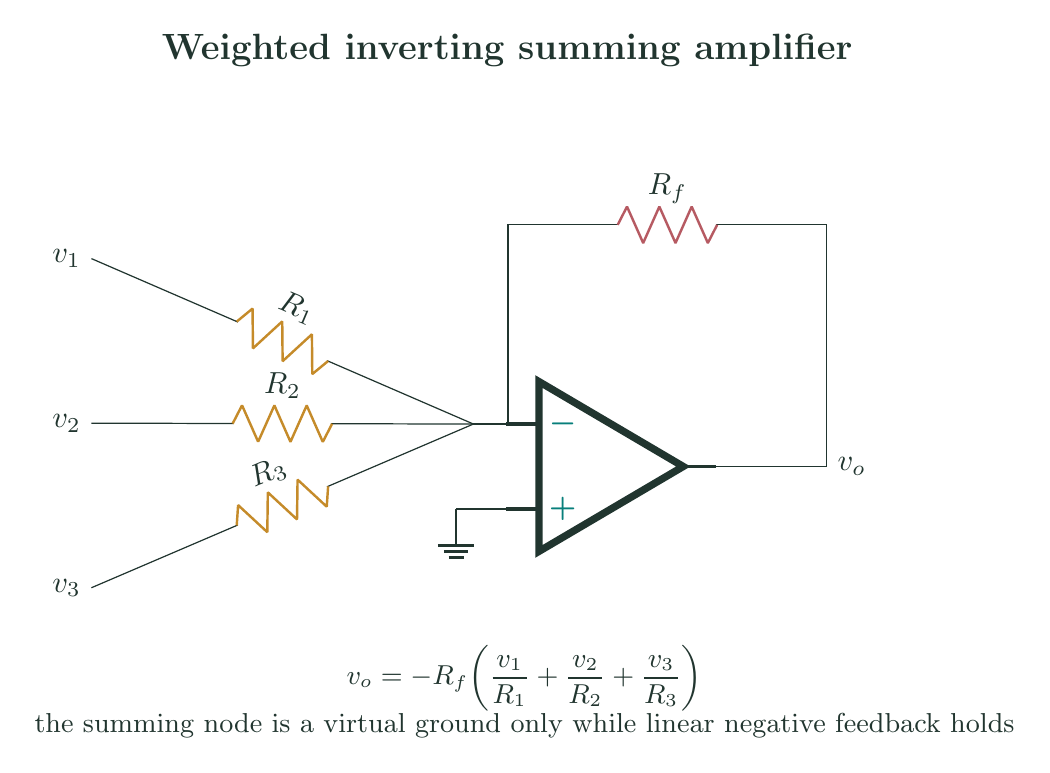
For equal input resistors $R_j=R$,
\[v_o=-\frac{R_f}{R}(v_1+v_2+\cdots+v_n).\]Choosing $R_f=R$ gives the negative sum. A second unity-gain inverter produces a positive sum. Choosing $R_f=R/n$ gives the negative arithmetic mean,
\[\boxed{v_o=-\frac1n\sum_{j=1}^{n}v_j}.\]Since the op amp sees all input branches in parallel when the independent sources are set to zero, the feedback factor is
\[\beta=\frac{R_p}{R_p+R_f},\qquad R_p=R_1\parallel R_2\parallel\cdots\parallel R_n,\]and the noise gain is
\[\boxed{G_N=1+\frac{R_f}{R_p}}.\]It can be much larger than any one signal coefficient. Noise, offset voltage and bandwidth must be evaluated using this noise gain.
Finite-open-loop-gain form
Let $v_+=0$ and $v_o=-Av_-$. KCL gives
\[\sum_j\frac{v_j-v_-}{R_j}+\frac{v_o-v_-}{R_f}=0.\]With $G=\sum_jR_j^{-1}$ and $I_s=\sum_jv_j/R_j$,
\[I_s-v_-G+\frac{-Av_--v_-}{R_f}=0.\]Therefore
\[v_- = \frac{I_s}{G+(A+1)/R_f}\]and
\[\boxed{ v_o=-\frac{A R_f}{A+1+R_fG} \sum_j\frac{v_j}{R_j} }.\]The ideal result is multiplied by $A/[A+1+R_fG]$. Since $1+R_fG=G_N$, the fractional gain error is governed by $G_N/A$, as expected.
Weighted-sum example
Take $R_f=20\,\text{k}\Omega$, $R_1=10\,\text{k}\Omega$, $R_2=20\,\text{k}\Omega$, $R_3=40\,\text{k}\Omega$, and
\[v_1=0.30\,\text{V},\quad v_2=-0.20\,\text{V},\quad v_3=0.80\,\text{V}.\]Then
\[v_o=-20\,\text{k}\Omega \left(\frac{0.30}{10\,\text{k}\Omega} -\frac{0.20}{20\,\text{k}\Omega} +\frac{0.80}{40\,\text{k}\Omega}\right) =-0.80\,\text{V}.\]The individual signal gains are $-2$, $-1$ and $-0.5$. Here
\[R_p=10\parallel20\parallel40\ \text{k}\Omega =5.714\,\text{k}\Omega,\]so $G_N=4.5$. An op amp with $f_t=9\,\text{MHz}$ has an approximate one-pole bandwidth $2\,\text{MHz}$ for this circuit, subject to parasitic capacitance and slew rate.
Four-resistor difference amplifier
In the difference amplifier, $v_1$ enters the inverting input through $R_1$ with feedback $R_2$, while $v_2$ drives a non-inverting divider $R_3,R_4$. Zero input current gives
\[v_+=\frac{R_4}{R_3+R_4}v_2.\]For an inverting stage referenced to $v_+$,
\[v_o=\left(1+\frac{R_2}{R_1}\right)v_+ -\frac{R_2}{R_1}v_1.\]Thus the general result is
\[\boxed{ v_o=\left(1+\frac{R_2}{R_1}\right) \frac{R_4}{R_3+R_4}v_2 -\frac{R_2}{R_1}v_1 }.\]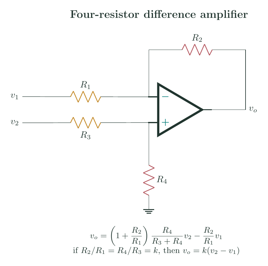
If
\[\boxed{\frac{R_2}{R_1}=\frac{R_4}{R_3}=k},\]then
\[\boxed{v_o=k(v_2-v_1)}.\]For $k=1$, all four resistors can be equal and the circuit is a unity-gain subtractor. For $k=10$, choices such as $R_1=R_3=10\,\text{k}\Omega$ and $R_2=R_4=100\,\text{k}\Omega$ produce $v_o=10(v_2-v_1)$.
Differential and common-mode gains
Write
\[v_1=v_{cm}-\frac{v_d}{2},\qquad v_2=v_{cm}+\frac{v_d}{2},\]where $v_d=v_2-v_1$. Define
\[a=\frac{R_2}{R_1},\qquad b=\left(1+a\right)\frac{R_4}{R_3+R_4}.\]The general output is $v_o=bv_2-av_1$, hence
\[v_o=(b-a)v_{cm}+\frac{a+b}{2}v_d.\]Therefore
\[\boxed{A_{cm}=b-a},\qquad \boxed{A_d=\frac{a+b}{2}},\]and
\[\boxed{\mathrm{CMRR}=\left\lvert\frac{A_d}{A_{cm}}\right\rvert}.\]Perfect ratio equality makes $a=b$ and cancels common mode in the ideal-resistor model. The op amp’s own finite CMRR then remains, but resistor mismatch often dominates.
Resistor-ratio mismatch
Suppose $a=k$ and the non-inverting ratio differs slightly so that $R_4/R_3=k(1+\epsilon)$. The exact $b$ is
\[b=(1+k)\frac{k(1+\epsilon)}{1+k(1+\epsilon)}.\]For $\lvert\epsilon\rvert\ll1$,
\[b-k\simeq\frac{k}{1+k}\epsilon,\]while $A_d\simeq k$. Thus
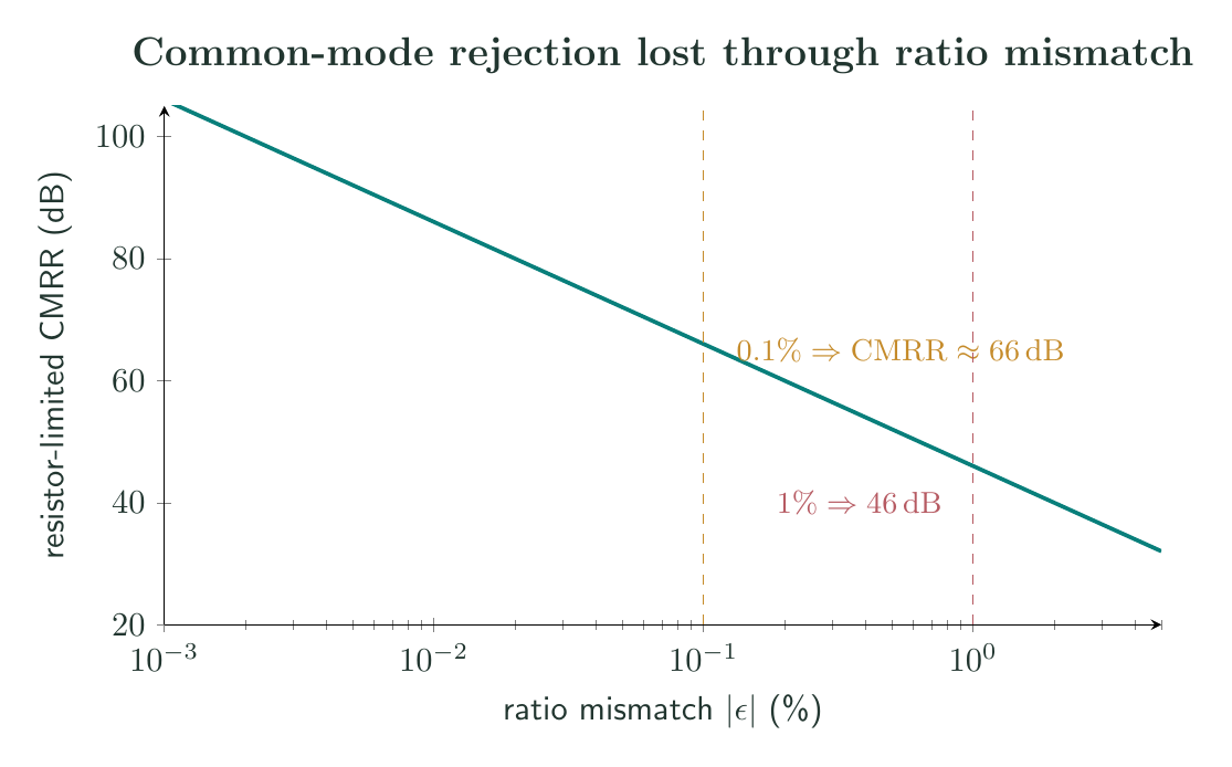
\[\boxed{\mathrm{CMRR}\simeq\frac{k+1}{\lvert\epsilon\rvert}}.\]For $k=1$ and ratio mismatch $\lvert\epsilon\rvert=0.001$, CMRR is approximately $2000$, or $66.0\,\text{dB}$. A $1\%$ mismatch reduces it to about $46\,\text{dB}$. These values describe the specified ratio mismatch, not necessarily the tolerance of a single resistor; worst-case ratio error can involve several resistor tolerances.
The common-mode input must lie inside the op amp’s allowed input range, and the required output $A_dv_d+A_{cm}v_{cm}$ must remain within its swing. A large common-mode voltage can therefore saturate the amplifier through a very small $A_{cm}$. The four-resistor circuit also has unequal and finite input resistances: the $v_1$ source sees approximately $R_1$, whereas the $v_2$ source sees $R_3+R_4$. When high and balanced input impedances are required, an instrumentation-amplifier input stage is used ahead of the subtractor.
Non-inverting weighted adder
Positive weighted sums can be formed at the non-inverting input. Suppose sources $v_j$ are connected through resistors $R_j$ to a node that also has resistance $R_g$ to a reference $V_R$. Since the op-amp input current is zero,
\[\sum_j\frac{v_j-v_+}{R_j} +\frac{V_R-v_+}{R_g}=0.\]Consequently,
\[\boxed{ v_+=\frac{\displaystyle\sum_jv_j/R_j+V_R/R_g} {\displaystyle\sum_j1/R_j+1/R_g} }.\]A non-inverting feedback stage then produces
\[v_o=\left(1+\frac{R_f}{R_1}\right)v_+.\]The node voltage is a conductance-weighted average, not a sum, before the non-inverting gain is applied. The sources load one another through the resistor network; therefore this form is unsuitable when source impedances are large or poorly known unless each source is buffered.
Binary-weighted conversion
An inverting summer can act as a simple digital-to-analog converter. If logic voltages $b_jV_H$, with $b_j\in{0,1}$, are applied through $R,2R,4R,\ldots,2^{n-1}R$ and $R_f=R$, then
\[v_o=-V_H\left(b_0+\frac{b_1}{2} +\frac{b_2}{4}+\cdots+\frac{b_{n-1}}{2^{n-1}}\right).\]The resistor spread grows as $2^{n-1}$, so tolerance, switch resistance and logic-output resistance limit accuracy at large $n$. An $R$–$2R$ ladder avoids this wide resistance range. The op-amp settling time must include both closed-loop dynamics and the code-dependent transient at the summing node.
Finite bandwidth with several inputs
Superposition remains valid for complex impedances. Replacing $R_j$ by $Z_j(s)$ and $R_f$ by $Z_f(s)$ gives, in the ideal op-amp limit,
\[\boxed{V_o(s)=-Z_f(s)\sum_j\frac{V_j(s)}{Z_j(s)}}.\]This expression describes weighted active filters as well as adders. However, the noise gain is
\[G_N(s)=1+Z_f(s)\sum_j\frac1{Z_j(s)},\]so reactive input branches can produce noise-gain peaks and poor phase margin. Signal-source impedances belong inside the corresponding $Z_j$.
For dc design, the maximum possible sum must be checked before choosing resistor ratios. If each of four equal-gain inputs can reach $2\,\text{V}$ and all have the same polarity, a gain of $-2$ requires $-16\,\text{V}$ output, which is impossible from many $\pm15\,\text{V}$ op-amp circuits after allowing output headroom. Linearity of the algebraic formula does not prevent saturation of its physical realization.
Combined common-mode rejection
The difference circuit has resistor-limited CMRR and the op amp has intrinsic CMRR. Their input-referred common-mode errors generally add rather than allowing the larger numerical CMRR to dominate. If $A_{cm,R}$ is produced by resistor mismatch and the op amp contributes approximately $A_d/\mathrm{CMRR}_{op}$, a conservative total is
\[\lvert A_{cm,tot}\rvert\leq \lvert A_{cm,R}\rvert +\frac{\lvert A_d\rvert}{\mathrm{CMRR}_{op}}.\]Thus
\[\mathrm{CMRR}_{tot}=\left\lvert\frac{A_d}{A_{cm,tot}}\right\rvert\]cannot exceed either limitation by design assumption alone. Frequency dependence matters because op-amp CMRR commonly falls with frequency while resistor ratios may acquire mismatch from parasitic capacitance.
Bias-current compensation and noise
In an inverting summer, the dc resistance seen at the inverting input with all ideal voltage sources set to zero is
\[R_T=R_f\parallel R_1\parallel R_2\parallel\cdots\parallel R_n.\]A resistor $R_T$ from the non-inverting input to ground cancels the average-bias-current contribution when the two input currents are equal. It does not cancel input offset current or voltage offset. Each input resistor also contributes thermal-current noise $4k_BT/R_j$ at the summing node, and the feedback resistor contributes its own noise. The output noise is not found by inserting rms source-noise voltages directly into the signed dc-sum formula unless their statistical independence is handled correctly; independent noise powers add.
For the difference amplifier, bias-current cancellation requires equality of the two dc Thevenin resistances as well as equality of signal-gain ratios. Under the matched-ratio condition $R_2/R_1=R_4/R_3=k$, the inverting resistance is $R_1\parallel R_2$ and the non-inverting resistance is $R_3\parallel R_4$. They are equal only when the absolute base resistors satisfy $R_1=R_3$. Ratio matching alone gives correct ideal subtraction, whereas simultaneous ratio and Thevenin-resistance matching minimizes both common-mode and bias-current errors.
Preparation questions
- Derive the finite-$A$ transfer expression of an $n$-input inverting summer and identify its noise gain.
- Design a three-input circuit for $v_o=-(2v_1+0.5v_2+4v_3)$ using $R_f=100\,\text{k}\Omega$.
- Show how an equal-resistor summer can be converted into an arithmetic averager.
- Derive the general four-resistor difference-amplifier output without assuming ratio matching.
- Starting from $v_1=v_{cm}-v_d/2$ and $v_2=v_{cm}+v_d/2$, obtain $A_d$ and $A_{cm}$.
- Estimate the output error caused by $10\,\text{V}$ common mode in a unity difference amplifier with $0.1\%$ ratio mismatch.


Discussion