

07 Jun 2025
Operational-Amplifier Architecture and Open-Loop Operation
Functional block diagram, internal differential and voltage-gain stages, level translation, output buffering, open-loop configurations, saturation and frequency response.
An operational amplifier is a direct-coupled, very-high-gain differential voltage amplifier designed to be used with an external feedback network. Its two input terminals are the non-inverting input $v_+$ and inverting input $v_-$. Define
\[v_d\equiv v_+-v_-.\]In the unsaturated low-frequency open-loop region,
\[\boxed{v_o=A_{OL}v_d},\]where $A_{OL}$ is positive under this sign convention. Increasing $v_+$ relative to $v_-$ drives the output positive. A real op-amp also responds weakly to the common-mode voltage $(v_++v_-)/2$, has finite input and output resistances, finite bandwidth, input offsets and limited output current.
Functional block diagram
The large open-loop gain is distributed among several stages rather than produced by one transistor pair. The functional partition is common to many voltage-feedback op-amps even though the detailed transistor circuits differ.
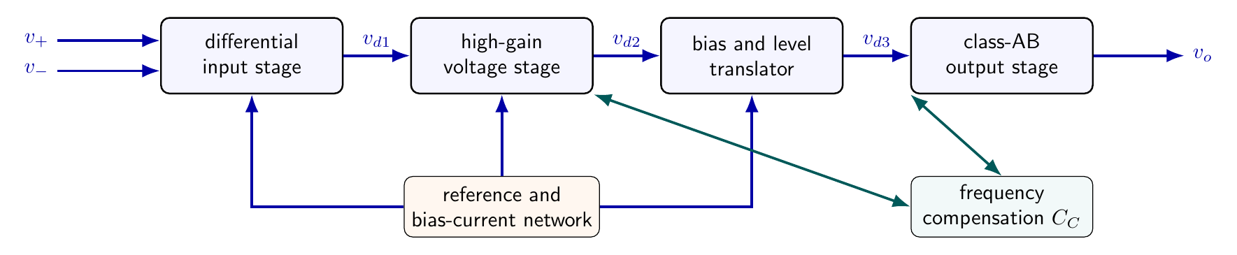
The differential input stage provides high input resistance, amplifies $v_+-v_-$ and suppresses common-mode signal. It also determines much of the input bias current, offset voltage, input noise and permitted common-mode range. A current-source tail and current-mirror active load give large CMRR and convert the differential collector currents to a single-ended signal.
The voltage-amplifier stage supplies most of the open-loop voltage gain. It commonly uses a transistor common-emitter stage with an active load, so its output node has large resistance. Because that node is high impedance, it also forms an important low-frequency pole when connected to the compensation capacitor.
The bias and level-translator network establishes nearly supply-independent currents and moves the DC signal level to the value required by the output stage. Translation must preserve the AC signal while compensating the base-emitter junction drops of the later transistors.
The output stage supplies load current and reduces output resistance. A complementary class-AB emitter-follower arrangement provides positive and negative current with a small quiescent current. Its voltage gain is close to unity, so it contributes little to $A_{OL}$ but substantially improves power-driving ability.
The frequency-compensation network, often dominated by an internal Miller capacitor $C_C$, intentionally creates a low-frequency dominant pole. It reduces open-loop gain before higher-frequency poles produce excessive phase lag.
Simplified transistor-level signal path
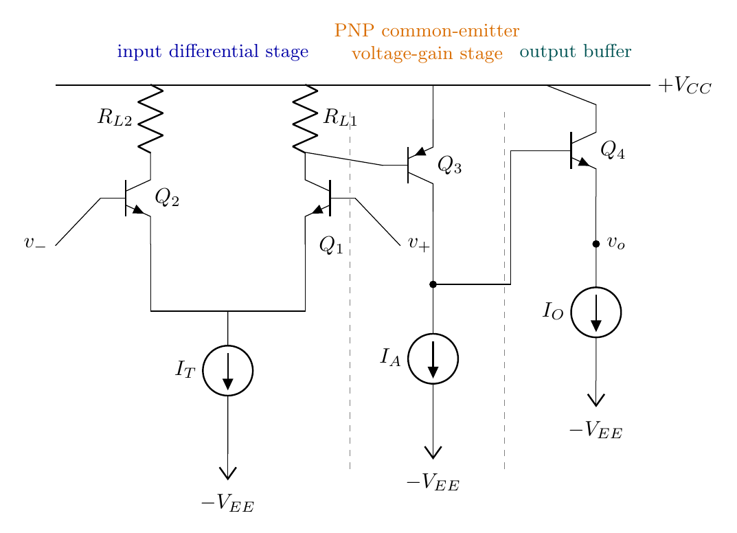
The following diagram is a pedagogical architecture rather than the complete circuit of a particular integrated op-amp. A commercial device contains current mirrors, protection circuits, startup networks and a complementary output stage in addition to the illustrated signal path.
If the low-frequency gains of successive stages are $A_1,A_2,\ldots,A_n$, the unloaded cascade gain is approximately
\[A_0\simeq A_1A_2\cdots A_n.\]The signs must be counted: each common-emitter stage inverts, whereas an emitter follower does not. In the illustrated circuit, increasing $v_+$ increases $Q_1$ current and lowers its collector voltage. The PNP common-emitter stage inverts this change, so its collector and the non-inverting $Q_4$ emitter follower move positively. The complete transfer therefore has the required sign, $v_o=A_0(v_+-v_-)$. Loading makes the actual product smaller because the input resistance of one stage appears in the output load of the preceding stage.
For the illustrated resistor-loaded differential input stage, with its single-ended signal taken from the $Q_1$ collector, a useful estimate is
\[A_1\simeq-\frac{g_{m1}}{2} \left(R_{L1}\parallel r_{o1}\parallel R_{in,3}\right).\]The emitter of PNP transistor $Q_3$ is connected to the positive rail, which is AC ground, while $I_A$ presents a large incremental resistance at its collector. Its common-emitter gain is therefore
\[A_2\simeq-g_{m3} \left(r_{o3}\parallel r_{o,I_A}\parallel R_{in,4}\right).\]Both $A_1$ and $A_2$ are negative, so their cascade is positive; the emitter-follower output buffer preserves that sign. A current-mirror-loaded input stage instead has an intrinsic gain magnitude of order $g_m(r_{o,n}\parallel r_{o,p})$. The translator and output buffer ordinarily have gains just below unity. Open-loop gains of $10^5$ to $10^6$ are possible at low frequency, but they are not maintained over a broad band.
Ideal and real terminal properties
An ideal voltage op-amp has
\[A_{OL}\to\infty, \qquad R_{in}\to\infty, \qquad R_o\to0,\]infinite bandwidth, infinite slew rate, zero input offset, zero bias currents and infinite CMRR. These are limiting assumptions, not properties that hold for an open-loop physical device.
A practical op-amp can be represented at low frequency by
\[v_o=A_d(v_+-v_-)+A_{cm}v_{cm}+V_{oo},\]before output limiting, where $V_{oo}$ represents output-referred offset. Equivalently, input offset voltage $V_{OS}$ can be placed in series with one input:
\[v_o\simeq A_d(v_d+V_{OS})+A_{cm}v_{cm}.\]Because $A_d$ is extremely large, microvolt input errors can produce volts of open-loop output.
The input common-mode range and output swing are separate restrictions. The input differential pair must keep its tail source and active loads in their intended regions, while the output stage must retain junction voltage and current headroom. Consequently an input voltage can be inside the supply rails yet outside the permitted common-mode range, and the output usually cannot reach either rail unless the device is specifically designed for rail-to-rail operation.
Open-loop configurations
Three input connections are possible without an external feedback path. In differential operation both terminals are driven independently. In open-loop inverting operation the non-inverting terminal is grounded and the signal is applied to $v_-$. In open-loop non-inverting operation $v_-$ is grounded and the signal is applied to $v_+$.
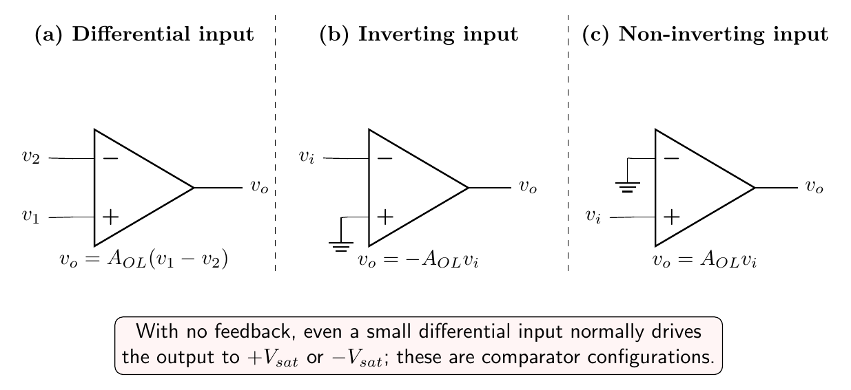
The ideal unsaturated relations are
\[\begin{aligned} \text{differential:}\quad &v_o=A_{OL}(v_1-v_2),\\ \text{inverting:}\quad &v_o=-A_{OL}v_i,\\ \text{non-inverting:}\quad &v_o=+A_{OL}v_i. \end{aligned}\]The output cannot exceed the limits set by the supplies and output-stage voltage drops. A static piecewise model is
\[v_o= \begin{cases} +V_{sat}, & A_0v_d>+V_{sat},\\ A_0v_d, & \lvert A_0v_d\rvert\le V_{sat},\\ -V_{sat}, & A_0v_d<-V_{sat}. \end{cases}\]The open-loop linear input interval is only
\[\boxed{\lvert v_d\rvert\le\frac{V_{sat}}{A_0}}.\]For $A_0=2.0\times10^5$ and $V_{sat}=14\ \mathrm V$, it is about $\pm70\ \mathrm{\mu V}$. Input offset voltage and noise are often comparable with this scale, so maintaining an open-loop output at an arbitrary intermediate voltage is impractical.
As a comparator, the sign of $v_d$ is the desired information. However, a general-purpose compensated op-amp is not necessarily an ideal fast comparator: recovery from deep saturation may be slow, input differential voltage may be restricted, and the output logic levels and switching speed may be unsuitable.
Open-loop frequency response
The simplest compensated model has one dominant pole:
\[\boxed{ A_{OL}(s)=\frac{A_0}{1+s/\omega_p} }.\]At $s=j\omega$,
\[\lvert A_{OL}(j\omega)\rvert= \frac{A_0}{\sqrt{1+(\omega/\omega_p)^2}},\] \[\angle A_{OL}(j\omega)=-\tan^{-1}\!\left(\frac{\omega}{\omega_p}\right).\]Above the dominant pole, the magnitude falls approximately as $1/f$, or $-20\ \mathrm{dB/decade}$. The unity-gain or transition frequency is approximately
\[\boxed{f_T\simeq A_0 f_p}.\]This product is the gain-bandwidth product for the one-pole region. Additional poles invalidate the single-pole expression near sufficiently high frequency and add phase lag.
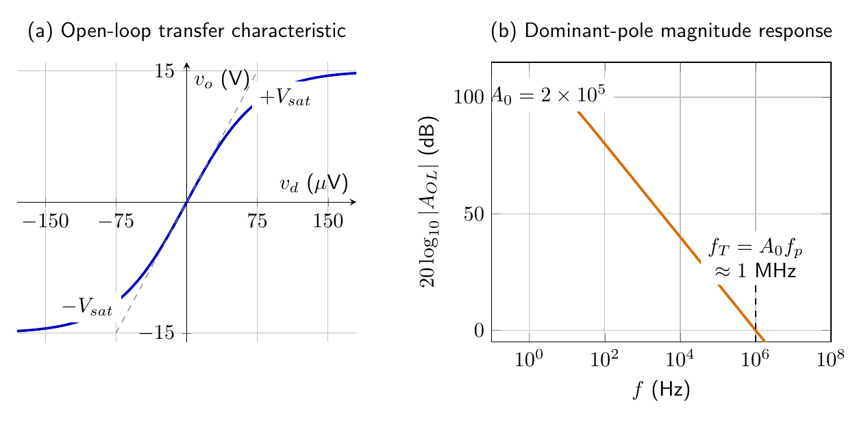
The small-signal frequency response assumes infinitesimal perturbations about a valid operating point. Large-signal operation has an additional slew-rate limit. If an internal compensation capacitor is charged by a maximum current $I_{max}$,
\[\left\lvert\frac{dv_o}{dt}\right\rvert_{max}=\mathrm{SR}\simeq\frac{I_{max}}{C_C}\]after allowance for the stage scaling. For a sine wave $v_o=V_p\sin\omega t$, avoiding slew-induced distortion requires
\[2\pi fV_p\le\mathrm{SR}.\]Slew rate and small-signal bandwidth are physically distinct specifications.
Cascaded-gain example
Suppose the differential stage gain is $80$, the voltage-amplifier stage gain is $2500$, the level translator has magnitude $0.98$ and the output buffer has magnitude $0.995$. Taking the internal stage polarities to give the standard positive overall sign,
\[A_0=(80)(2500)(0.98)(0.995)=1.9502\times10^5,\]or
\[20\log_{10}A_0=105.8\ \mathrm{dB}.\]For a dominant pole $f_p=5.0\ \mathrm{Hz}$,
\[f_T=A_0f_p=9.751\times10^5\ \mathrm{Hz}.\]At $f=10\ \mathrm{kHz}$,
\[\lvert A_{OL}\rvert= \frac{1.9502\times10^5}{\sqrt{1+(10^4/5)^2}} =97.51,\]and the phase is approximately $-89.97^\circ$. With $V_{sat}=14\ \mathrm V$, saturation begins at
\[\lvert v_d\rvert=\frac{14}{1.9502\times10^5} =71.8\ \mathrm{\mu V}\]at low frequency. A DC differential input of $25\ \mathrm{\mu V}$ ideally produces $4.88\ \mathrm V$ and remains inside this static range, whereas $100\ \mathrm{\mu V}$ would demand $19.5\ \mathrm V$ and force saturation.
Preparation questions
- Draw and explain the functional block diagram of a voltage-feedback operational amplifier, identifying the principal specification controlled by each stage.
- Explain how the differential stage, active load, voltage-amplifier stage, level translator and output buffer form a complete signal path.
- Distinguish differential, open-loop inverting and open-loop non-inverting configurations and derive their output polarities.
- Why is an uncompensated or compensated op-amp generally unsuitable as a precision linear amplifier in open loop?
- Starting with a dominant-pole transfer function, derive the Bode magnitude, phase and unity-gain frequency.
- An op-amp has $A_0=3\times10^5$, $f_p=8\ \mathrm{Hz}$ and $V_{sat}=13\ \mathrm V$. Calculate $f_T$, the gain at $20\ \mathrm{kHz}$ and the low-frequency differential input that initiates saturation.
- Distinguish the gain-bandwidth limit from the slew-rate limit for a sinusoidal output.


Discussion