

13 Jul 2026
Single-Stage RC-Coupled Transistor Amplifier in CE Mode
Aim
To study the voltage gain and frequency response of a single-stage RC-coupled transistor amplifier in common-emitter mode.
Apparatus
NPN transistor, DC supply, bias resistors, collector resistor, coupling capacitors, function generator, CRO, and connecting leads.
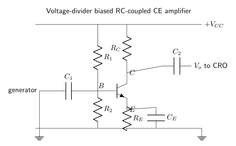
Experimental arrangement
Theory
A transistor amplifier must first be biased at a quiescent operating point in the active region. The voltage divider $R_1$-$R_2$ fixes the base voltage, while $R_E$ introduces DC negative feedback: if collector current rises, the emitter voltage rises and reduces $V_{BE}$. The collector resistor converts variations of collector current into output-voltage variations.
The coupling capacitors pass the alternating signal but prevent the generator and load from disturbing the DC bias. During the positive half-cycle of the base signal, collector current increases and the voltage drop across $R_C$ increases. The collector voltage therefore falls, giving the characteristic $180^\circ$ phase reversal of a common-emitter stage.
For a small signal, $i_c=g_mv_{be}$, where $g_m=I_C/V_T$ and $V_T\approx25$ mV at room temperature. If the emitter is effectively bypassed, the mid-band gain is approximately
\[A_v=\frac{V_o}{V_i}\approx-g_m(R_C\parallel R_L).\]At low frequency, the reactances of $C_1$, $C_2$, and $C_E$ are appreciable and the gain falls. At high frequency, transistor junction capacitances and wiring capacitance reduce the gain. The cutoff frequencies satisfy $A_v=0.707A_{v,\text{mid}}$, and the bandwidth is $BW=f_H-f_L$.
Observations
| Frequency (kHz) | Input (mV) | Output (V) | Gain $A_v$ |
|---|---|---|---|
| 0.05 | 20 | 0.84 | 42.0 |
| 0.10 | 20 | 1.12 | 56.0 |
| 1.0 | 20 | 1.20 | 60.0 |
| 10 | 20 | 1.14 | 57.0 |
| 100 | 20 | 0.80 | 40.0 |
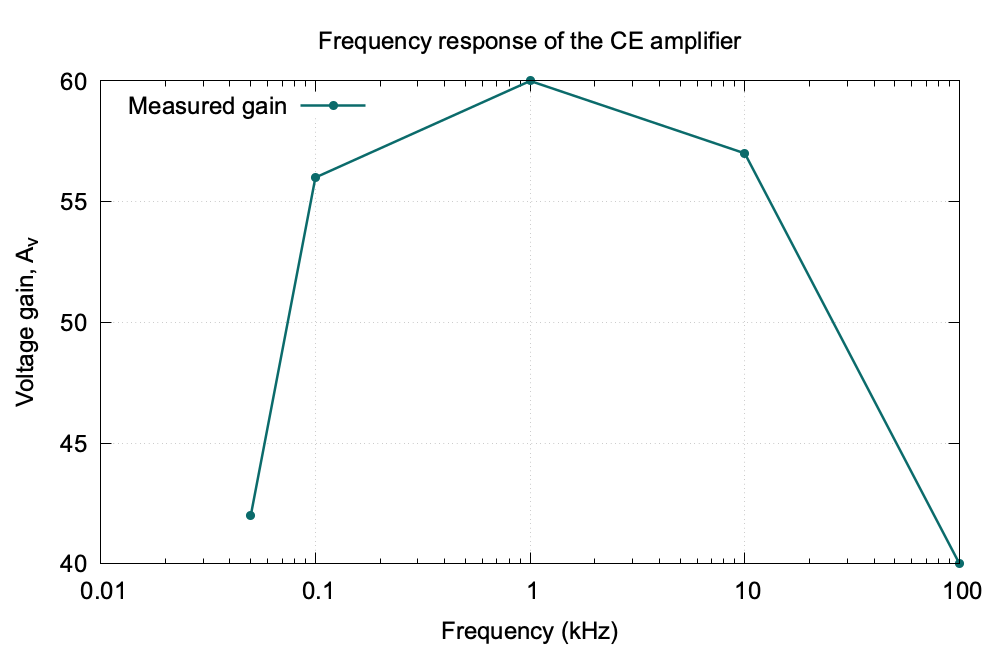
Graph
Calculation
At 1 kHz,
\[A_v=\frac{V_o}{V_i}=\frac{1.20}{20\times10^{-3}}=60.\]The half-power gain is $0.707(60)=42.4$. The observations place the lower and upper cutoffs close to 0.05 kHz and 100 kHz respectively. Hence the approximate bandwidth is
\[BW=f_H-f_L=100-0.05=99.95\,\text{kHz}.\]Result
The amplifier gives a mid-band voltage gain of approximately $60$. The gain decreases at low and high frequencies because of coupling/bypass capacitors and transistor stray capacitances.
Viva Questions
- Why is the output phase reversed? An increase in collector current increases the voltage drop across the collector resistor and lowers the collector voltage.
- What is bandwidth? The difference between upper and lower half-power frequencies.
- Why is the emitter bypassed in a practical amplifier? To reduce AC negative feedback and increase voltage gain.


Discussion