

13 Jul 2026
Drain and Transfer Characteristics of a JFET
Aim
To study the drain and transfer characteristics of a junction field-effect transistor and determine its transconductance.
Apparatus
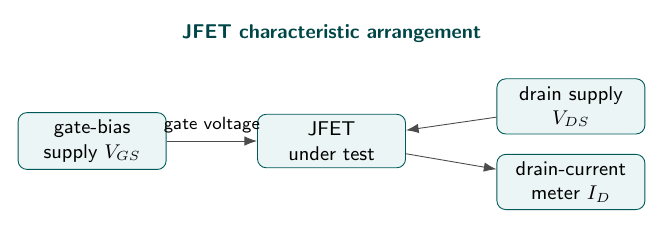
JFET, regulated DC supplies, milliammeter, voltmeters, bias resistors, and connecting leads.
Figure
Theory
An n-channel JFET consists of an n-type channel between source and drain and p-type gate regions forming reverse-biased p-n junctions with that channel. Electrons entering the source drift towards the drain when $V_{DS}$ is positive. Since the gate junction is reverse biased, its current is nearly zero; the device is controlled by the electric field of the depletion layers rather than by an input current.
For small $V_{DS}$ the channel behaves approximately as a voltage-controlled resistance, so $I_D$ initially rises with $V_{DS}$. The reverse bias is greatest near the drain, making the channel narrower there. When the depletion layers nearly meet, the channel is pinched near the drain. Further increase of $V_{DS}$ mainly extends the pinched region and $I_D$ becomes almost constant. This is the saturation or pinch-off region used for the transfer characteristic.
Making $V_{GS}$ more negative widens the depletion layers throughout the channel and reduces $I_D$. At $V_{GS}=V_P$ the channel is cut off. In saturation the transfer characteristic is approximated by Shockley’s equation,
\[I_D=I_{DSS}\left(1-\frac{V_{GS}}{V_P}\right)^2.\]Here $I_{DSS}$ is the saturation current at $V_{GS}=0$ and $V_P$ is the negative gate voltage at cutoff. The transconductance measures the control of drain current by gate voltage:
\[g_m=\left.\frac{\partial I_D}{\partial V_{GS}}\right|_{V_{DS}}.\]It is obtained experimentally from the slope of the $I_D$-$V_{GS}$ graph at constant $V_{DS}$.
Observations
| $V_{DS}$ (V) | $I_D$ at $V_{GS}=0$ (mA) | $I_D$ at $V_{GS}=-1$ V (mA) |
|---|---|---|
| 2 | 4.1 | 2.8 |
| 4 | 5.0 | 3.1 |
| 6 | 5.2 | 3.2 |
| 8 | 5.3 | 3.2 |
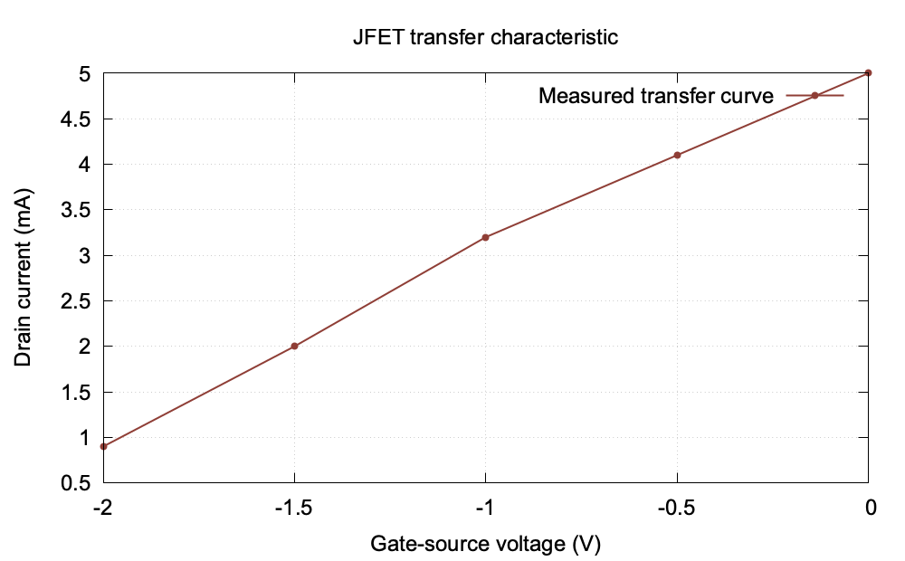
Transfer readings at $V_{DS}=6$ V:
| $V_{GS}$ (V) | 0.0 | -0.5 | -1.0 | -1.5 | -2.0 |
|---|---|---|---|---|---|
| $I_D$ (mA) | 5.2 | 4.1 | 3.2 | 2.0 | 0.9 |
Graph
Calculation
At $V_{DS}=6$ V, the table gives $I_D=5.2$ mA at $V_{GS}=0$ and $I_D=3.2$ mA at $V_{GS}=-1$ V. Therefore the mean transconductance over this interval is
\[g_m\approx\frac{5.2-3.2}{0-(-1)}=2.0\,\text{mA V}^{-1}=2.0\,\text{mS}.\]Result
The drain current becomes nearly constant after pinch-off. The transconductance over the measured interval near $V_{GS}=-1$ V is approximately $2.0$ mS.
Viva Questions
- Why is gate current small? The gate junction is reverse biased.
- What is pinch-off? The condition in which the channel narrows enough for drain current to become nearly constant.
- What is transconductance? $g_m=\Delta I_D/\Delta V_{GS}$ at constant $V_{DS}$.


Discussion