

13 Jul 2026
Verification of Half Adder and Full Adder Circuits
Aim
To construct and verify half-adder and full-adder circuits using basic logic gates.
Apparatus
Digital trainer, XOR, AND, OR, and NAND ICs, regulated $5$ V supply, switches, LEDs, and patch cords.
Experimental arrangement
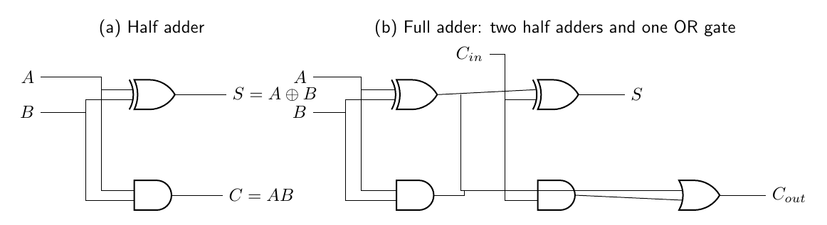
Theory
Binary numbers are added from the least significant column towards the most significant column. In one column, the arithmetic total can be 0, 1, 2, or 3. The sum output records the least significant bit of this total, while the carry output records whether the total is at least 2.
A half adder adds only $A$ and $B$. Its sum is one for unlike inputs and its carry is one only when both inputs are one:
\[S=A\oplus B,\qquad C=AB.\]It cannot accept a carry from a preceding column. A full adder therefore has the third input $C_{in}$. The first half adder forms $S_1=A\oplus B$ and $C_1=AB$. The second adds $S_1$ and $C_{in}$, giving $S=S_1\oplus C_{in}$ and $C_2=S_1C_{in}$. ORing the two carry terms gives
\(S=A\oplus B\oplus C_{in},\) \(C_{out}=AB+C_{in}(A\oplus B).\)
Equivalent full-adder stages can be cascaded to add multi-bit numbers. Each stage must wait for the carry from the preceding stage, producing the ripple-carry propagation delay.
Observations
| $A$ | $B$ | $C_{in}$ | Sum $S$ | Carry $C_{out}$ |
|---|---|---|---|---|
| 0 | 0 | 0 | 0 | 0 |
| 0 | 1 | 0 | 1 | 0 |
| 1 | 0 | 1 | 0 | 1 |
| 1 | 1 | 0 | 0 | 1 |
| 1 | 1 | 1 | 1 | 1 |
Verification
For $A=B=C_{in}=1$, the arithmetic sum is $1+1+1=3=112$. Therefore $S=1$ and $C{out}=1$. The Boolean equations give the same result:
\[S=1\oplus1\oplus1=1,\] \[C_{out}=(1)(1)+(1)(1\oplus1)=1+0=1.\]Result
The observed outputs agree with the truth tables of the half adder and full adder.
Viva Questions
- Why does a full adder need three inputs? It adds two data bits and the carry from the preceding stage.
- What is the half-adder carry expression? $C=AB$.
- How can a full adder be made from half adders? Use two half adders followed by an OR gate for their carry outputs.


Discussion