

13 Jul 2026
Drain and Transfer Characteristics of an Enhancement MOSFET
Aim
To obtain the drain and transfer characteristics of an n-channel enhancement MOSFET and determine its threshold voltage and transconductance.
Apparatus
Enhancement MOSFET, regulated gate and drain supplies, milliammeter, voltmeters, resistors, breadboard, and connecting leads.
Experimental arrangement
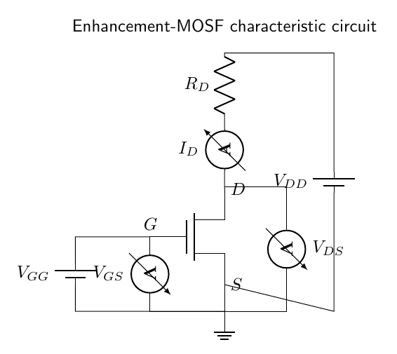
Theory
An n-channel enhancement MOSFET has two n-type regions, source and drain, separated by a p-type body. The metal gate is insulated from the semiconductor by a thin oxide, so the steady gate current is practically zero. At $V_{GS}=0$ there is no n-type path between source and drain and the device is normally off.
A positive gate voltage produces an electric field through the oxide. Holes are repelled from the surface and electrons are attracted towards it. When the surface electron concentration becomes sufficient, an inversion layer joins source and drain. The gate voltage at which this conducting channel is established is the threshold voltage $V_T$.
For $V_{GS}>V_T$ and small $V_{DS}$, the device operates in the ohmic region and behaves as a gate-controlled resistor. As $V_{DS}$ approaches $V_{GS}-V_T$, the channel pinches near the drain. Beyond this condition the device enters saturation and the ideal square-law relation is
\[I_D=K(V_{GS}-V_T)^2,\]where $K$ depends on oxide capacitance, channel dimensions, and carrier mobility. The transconductance is the slope of the transfer characteristic at constant $V_{DS}$:
\[g_m=\frac{dI_D}{dV_{GS}}=2K(V_{GS}-V_T).\]The threshold is estimated from the onset of current or, more accurately, from the intercept of a straight-line plot of $\sqrt{I_D}$ against $V_{GS}$.
Observations
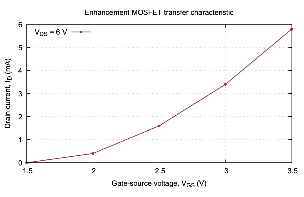
| $V_{GS}$ (V) | $I_D$ (mA) at $V_{DS}=6$ V |
|---|---|
| 1.5 | 0.0 |
| 2.0 | 0.4 |
| 2.5 | 1.6 |
| 3.0 | 3.4 |
| 3.5 | 5.8 |
Graph
Calculation
The current first becomes measurable between 1.5 V and 2.0 V, giving the experimental estimate $V_T\approx1.9$ V. Around $V_{GS}=3.0$ V, a central-difference estimate gives
\[g_m\approx\frac{I_D(3.5)-I_D(2.5)}{3.5-2.5}=\frac{5.8-1.6}{1.0}=4.2\,\text{mS}.\]Result
The threshold voltage from the onset of drain current is approximately $V_T=1.9$ V. The drain current increases quadratically with gate voltage in the saturation region.
Viva Questions
- Why is gate current nearly zero? The gate is insulated from the channel by a thin oxide layer.
- What is threshold voltage? The minimum gate-source voltage needed to form a conducting channel.
- Why must the MOSFET be protected from static charge? The thin gate oxide can be damaged by a large electrostatic voltage.


Discussion