

13 Jul 2026
Tunnelling Effect in a Tunnel Diode
practical
ug-vi
semiconductor
tunnel-diode
tunnelling
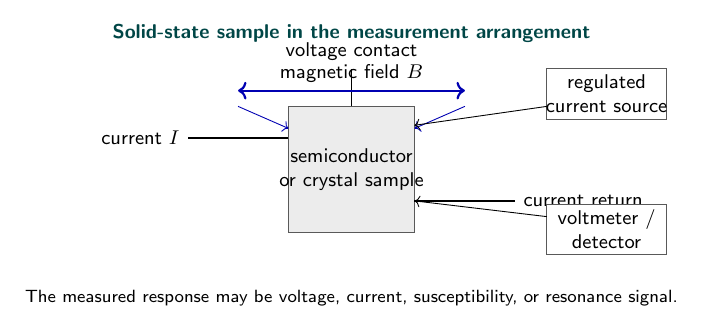
Experimental arrangement
Aim
To study the current-voltage characteristic of a tunnel diode and identify its negative-resistance region.
Apparatus
Tunnel diode, regulated supply, microammeter, voltmeter, series resistor, and connecting wires.
Theory
Heavy doping makes the depletion layer extremely thin, allowing carriers to tunnel through the barrier. The current first increases to a peak, then decreases with increasing voltage, and finally increases again by ordinary conduction. The negative differential resistance is
\[r_d=\frac{dV}{dI}<0.\]Observations
| Voltage (V) | Current (mA) |
|---|---|
| 0.00 | 0.0 |
| 0.05 | 1.8 |
| 0.10 | 3.4 |
| 0.15 | 2.6 |
| 0.20 | 1.4 |
| 0.30 | 2.0 |
| 0.40 | 4.2 |
Peak point: $(V_p,I_p)=(0.10\,\text{V},3.4\,\text{mA})$; valley point: $(V_v,I_v)=(0.20\,\text{V},1.4\,\text{mA})$.
Result
The negative-resistance region extends approximately from $0.10$ to $0.20\,\text{V}$.
Precautions
- Use a low-current range.
- Increase voltage in small steps near peak and valley points.
- Do not exceed the diode rating.
Viva Questions
- What causes tunnelling? Quantum-mechanical transmission through a very thin potential barrier.
- What is negative resistance? A region in which current decreases as voltage increases.
- Where are tunnel diodes used? High-frequency oscillators, switching circuits, and microwave devices.


Discussion